SBOS382H may 2008 – june 2023 OPA2673
PRODUCTION DATA
- 1
- 1 Features
- 2 Applications
- 3 Description
- 4 Revision History
- 5 Device Family Comparison Table
- 6 Pin Configuration and Functions
-
7 Specifications
- 7.1 Absolute Maximum Ratings
- 7.2 ESD Ratings
- 7.3 Recommended Operating Conditions
- 7.4 Thermal Information
- 7.5 Electrical Characteristics: Full Bias and Offline Mode VS = ±6 V
- 7.6 Electrical Characteristics: 75% Bias Mode VS = ±6 V
- 7.7 Electrical Characteristics: 50% Bias Mode VS = ±6 V
- 7.8 Typical Characteristics: VS = ±6 V, Full Bias
- 7.9 Typical Characteristics: VS = ±6 V Differential, Full Bias
- 7.10 Typical Characteristics: VS = ±6 V, 75% Bias
- 7.11 Typical Characteristics: VS = ±6 V, 50% Bias
- 8 Detailed Description
- 9 Application and Implementation
- 10Device and Documentation Support
- 11Mechanical, Packaging, and Orderable Information
Package Options
Mechanical Data (Package|Pins)
- RGV|16
Thermal pad, mechanical data (Package|Pins)
- RGV|16
Orderable Information
8.3.1.4 Line Driver Headroom Model
The first step in a driver design is to compute the peak-to-peak output voltage from the target specifications. This calculation is done using the following equations:
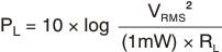
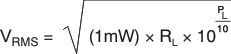
With PL power and VRMS voltage at the load, and RL load impedance, this calculation gives:

With VP peak voltage at the load and the crest factor, CF:

With VLPP: peak-to-peak voltage at the load.
Consolidating Equation 2 through Equation 5 allows the required peak-to-peak voltage at the load function of the crest factor, the load impedance, and the power in the load to be expressed. Thus:
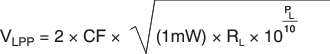
This VLPP is usually computed for a nominal line impedance and can be taken as a fixed design target.
The next step for the driver is to compute the individual amplifier output voltage and currents as a function of VPP on the line and transformer turns ratio. As the turns ratio changes, the minimum allowed supply voltage also changes. The peak current in the amplifier is given by:
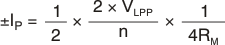
With VLPP defined in Equation 6 and RM defined in Equation 8.

The peak current is computed in Figure 8-9 by noting that the total load is 4RM and that the peak current is half of the peak-to-peak calculated using VLPP.
 Figure 8-9 Driver Peak
Output Model
Figure 8-9 Driver Peak
Output ModelWith the required output voltage and current versus turns ratio set, an output stage headroom model allows the required supply voltage versus turns ratio to be developed.
The headroom model (see Figure 8-10) can be described with the following set of equations:
First, as available output voltage for each amplifier:

Or, second, as required single-supply voltage:

The minimum supply voltage for a set of power and load requirements is given by Equation 10, where V1, V2, R1, and R2 are internal to the OPA2673.
Table 8-1 gives V1, V2, R1, and R2 for +12-V operation of the OPA2673.
 Figure 8-10 Line Driver
Headroom Model
Figure 8-10 Line Driver
Headroom Model| V1 | R1 | V2 | R2 |
|---|---|---|---|
| 0.9 V | 2 Ω | 0.9 V | 2 Ω |