SBOS233G March   2002  – April 2018 OPA2354 , OPA354 , OPA4354

PRODUCTION DATA.  

  1. Features
  2. Applications
  3. Description
    1.     Device Images
      1.      Simplified Schematic
  4. Revision History
  5. Device Comparison Table
  6. Pin Configuration and Functions
    1.     Pin Functions: OPA354
    2.     Pin Functions: OPA2354
    3.     Pin Functions: OPA4354
  7. Specifications
    1. 7.1 Absolute Maximum Ratings
    2. 7.2 ESD Ratings
    3. 7.3 Recommended Operating Conditions
    4. 7.4 Thermal Information: OPA354
    5. 7.5 Thermal Information: OPA2354
    6. 7.6 Thermal Information: OPA4354
    7. 7.7 Electrical Characteristics: VS = 2.7 V to 5.5 V (Single-Supply)
    8. 7.8 Typical Characteristics
  8. Detailed Description
    1. 8.1 Overview
    2. 8.2 Functional Block Diagram
    3. 8.3 Feature Description
      1. 8.3.1 Operating Voltage
      2. 8.3.2 Rail-to-Rail Input
      3. 8.3.3 Rail-to-Rail Output
      4. 8.3.4 Output Drive
      5. 8.3.5 Video
      6. 8.3.6 Driving Analog-to-Digital converters
      7. 8.3.7 Capacitive Load and Stability
      8. 8.3.8 Wideband Transimpedance Amplifier
    4. 8.4 Device Functional Modes
  9. Application and Implementation
    1. 9.1 Application Information
    2. 9.2 Typical Application
      1. 9.2.1 Design Requirements
      2. 9.2.2 Detailed Design Procedure
        1. 9.2.2.1 Optimizing the Transimpedance Circuit
      3. 9.2.3 Application Curve
  10. 10Power Supply Recommendations
  11. 11Layout
    1. 11.1 Layout Guidelines
    2. 11.2 Layout Example
    3. 11.3 Power Dissipation
    4. 11.4 PowerPAD Thermally-Enhanced Package
    5. 11.5 PowerPAD Assembly Process
  12. 12Device and Documentation Support
    1. 12.1 Documentation Support
    2. 12.2 Related Links
    3. 12.3 Receiving Notification of Documentation Updates
    4. 12.4 Community Resources
    5. 12.5 Trademarks
    6. 12.6 Electrostatic Discharge Caution
    7. 12.7 Glossary
  13. 13Mechanical, Packaging, and Orderable Information

Package Options

Mechanical Data (Package|Pins)
Thermal pad, mechanical data (Package|Pins)
Orderable Information

Output Drive

The OPAx354 output stage supplies a continuous output current of ±100 mA and yet provide approximately
2.7 V of output swing on a 5-V supply, as shown in Figure 30. For maximum reliability, TI does not recommend running a continuous DC current in excess of ±100 mA. See the typical characteristic curves, Output Voltage Swing vs Output Current (Figure 20 and Figure 22). For supplying continuous output currents greater than ±100 mA, the OPAx354 may be operated in parallel, as shown in Figure 31.
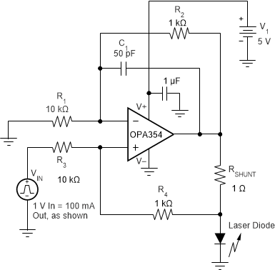
OPA354 OPA2354 OPA4354 ai_laser_diode_driver_bos233.gifFigure 30. Laser Diode Driver

The OPAx354 provides peak currents up to 200 mA, which corresponds to the typical short-circuit current. Therefore, an on-chip thermal shutdown circuit is provided to protect the OPAx354 from dangerously high junction temperatures. At 160°C, the protection circuit shuts down the amplifier. Normal operation resumes when the junction temperature cools to below 140°C.
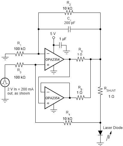
OPA354 OPA2354 OPA4354 ai_parallel_op_bos233.gifFigure 31. Parallel Operation