SBOS492F June 2009 – May 2018 OPA2354A-Q1 , OPA354A-Q1 , OPA4354-Q1
PRODUCTION DATA.
- 1 Features
- 2 Applications
- 3 Description
- 4 Revision History
- 5 Pin Configuration and Functions
- 6 Specifications
- 7 Detailed Description
- 8 Application and Implementation
- 9 Power Supply Recommendations
- 10Layout
- 11Device and Documentation Support
- 12Mechanical, Packaging, and Orderable Information
Package Options
Mechanical Data (Package|Pins)
- DBV|5
Thermal pad, mechanical data (Package|Pins)
Orderable Information
3 Description
The design of the OPAx354-Q1 family of high-speed, voltage-feedback CMOS operational amplifiers is for video and other applications requiring wide bandwidth. These devices are unity-gain stable and can drive large output currents. Differential gain is 0.02% and differential phase is 0.09°. Quiescent current is only 4.9 mA per channel.
The OPAx354-Q1 family of operational amplifiers (op-amps) are optimized for operation on single or dual supplies as low as 2.5 V (±1.25 V) and up to 5.5 V (±2.75 V). Common-mode input range extends beyond the supplies. The output swing is within 100 mV of the rails, supporting wide dynamic range.
The single-supply version (OPA354A-Q1) is available in the tiny SOT–23-5 (DBV) package. The dual-supply version (OPA2354A-Q1) is available in the miniature VSSOP-8 (DGK) package and features completely independent circuitry for lowest crosstalk and freedom from interaction. The quad-supply version (OPA4354-Q1) is available in the TSSOP-14 (PW) package. The device specifications are for operation over the automotive temperature range of –40°C to +125°C.
Device Information(1)
| PART NUMBER | PACKAGE (PIN) | BODY SIZE (NOM) |
|---|---|---|
| OPA354A-Q1 | SOT-23 (5) | 2.90 mm × 1.60 mm |
| OPA2354A-Q1 | VSSOP (8) | 3.00 mm × 3.00 mm |
| OPA4354-Q1 | TSSOP (14) | 5.00 mm × 4.40 mm |
- For all available packages, see the orderable addendum at the end of the data sheet.
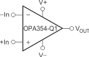
Simplified Schematic
