SBOS512E March   2010  – November 2020 OPA2365-Q1 , OPA365-Q1

PRODUCTION DATA  

  1. Features
  2. Applications
  3. Description
  4. Revision History
  5. Pin Configuration and Functions
  6. Specifications
    1. 6.1 Absolute Maximum Ratings
    2. 6.2 ESD Ratings
    3. 6.3 Recommended Operating Conditions
    4. 6.4 Thermal Information
    5. 6.5 Electrical Characteristics
    6. 6.6 Typical Characteristics
  7. Detailed Description
    1. 7.1 Overview
    2. 7.2 Functional Block Diagram
    3. 7.3 Feature Description
      1. 7.3.1 Operating Characteristics
      2. 7.3.2 Basic Amplifier Configurations
      3. 7.3.3 Input and ESD Protection
      4. 7.3.4 Rail-to-Rail Input
    4. 7.4 Device Functional Modes
  8. Application and Implementation
    1. 8.1 Application Information
      1. 8.1.1 Capacitive Loads
      2. 8.1.2 Achieving an Output Level of Zero Volts (0 V)
      3. 8.1.3 Active Filtering
      4. 8.1.4 Driving an ADS7822-Q1 Analog-to-Digital Converter
      5. 8.1.5 Driving ADS1115-Q1 Analog-to-Digital Converter
    2. 8.2 Typical Application
      1. 8.2.1 Fast Settling Peak Detector
        1. 8.2.1.1 Design Requirements
        2. 8.2.1.2 Detailed Design Procedure
        3. 8.2.1.3 Application Curves
      2. 8.2.2 Bandpass Filter 1.5 kHz to 160 kHz and 40-db Flat Gain
        1. 8.2.2.1 Design Requirements
        2. 8.2.2.2 Detailed Design Procedure
        3. 8.2.2.3 Application Curves
  9. Power Supply Recommendations
  10. 10Layout
    1. 10.1 Layout Guidelines
    2. 10.2 Layout Example
  11. 11Device and Documentation Support
    1. 11.1 Documentation Support
      1. 11.1.1 Related Documentation
    2. 11.2 Support Resources
    3. 11.3 Trademarks
    4. 11.4 Electrostatic Discharge Caution
    5. 11.5 Glossary
  12. 12Mechanical, Packaging, and Orderable Information

Package Options

Mechanical Data (Package|Pins)
Thermal pad, mechanical data (Package|Pins)
Orderable Information

Driving an ADS7822-Q1 Analog-to-Digital Converter

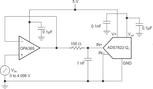
The OPAx365-Q1 operational amplifiers are optimized for driving medium to high speed sampling A/D converters. The OPAx365-Q1 op amps buffer the A/D’s input capacitance and resulting charge injection while providing signal gain. Figure 8-5 shows the OPAx365-Q1 in a basic noninverting configuration driving the ADS7822-Q1. The ADS7822-Q1 is a 12-bit, micro-power sampling converter in the MSOP-8 package. When used with the low-power, miniature packages of the OPAx365-Q1, the combination is ideal for space-limited, low power applications. In this configuration, an RC network at the A/D’s input can be used to filter charge injection.
GUID-495A4148-0D23-4F3D-A43F-3C5371147877-low.gifFigure 8-5 Driving the ADS7822-Q1