SBOS618I December   2013  – May 2018 OPA172 , OPA2172 , OPA4172

PRODUCTION DATA.  

  1. Features
  2. Applications
  3. Description
    1.     Device Images
      1.      JFET-Input Low-Noise Amplifier
      2.      Superior THD Performance
  4. Revision History
  5. Device Comparison
    1. 5.1 Device Comparison
    2. 5.2 Device Family Comparison
  6. Pin Configuration and Functions
    1.     Pin Functions: OPA172
    2.     Pin Functions: OPA2172 and OPA4172
  7. Specifications
    1. 7.1 Absolute Maximum Ratings
    2. 7.2 ESD Ratings
    3. 7.3 Recommended Operating Conditions
    4. 7.4 Thermal Information: OPA172
    5. 7.5 Thermal Information: OPA2172
    6. 7.6 Thermal Information: OPA4172
    7. 7.7 Electrical Characteristics
    8. 7.8 Typical Characteristics: Table of Graphs
    9. 7.9 Typical Characteristics
  8. Detailed Description
    1. 8.1 Overview
    2. 8.2 Functional Block Diagram
    3. 8.3 Feature Description
      1. 8.3.1 EMI Rejection
      2. 8.3.2 Phase-Reversal Protection
      3. 8.3.3 Capacitive Load and Stability
    4. 8.4 Device Functional Modes
      1. 8.4.1 Common-Mode Voltage Range
      2. 8.4.2 Electrical Overstress
      3. 8.4.3 Overload Recovery
  9. Applications and Implementation
    1. 9.1 Application Information
    2. 9.2 Typical Applications
      1. 9.2.1 Capacitive Load Drive Solution Using an Isolation Resistor
        1. 9.2.1.1 Design Requirements
        2. 9.2.1.2 Detailed Design Procedure
        3. 9.2.1.3 Application Curve
      2. 9.2.2 Bidirectional Current Source
      3. 9.2.3 JFET-Input Low-Noise Amplifier
  10. 10Power-Supply Recommendations
  11. 11Layout
    1. 11.1 Layout Guidelines
    2. 11.2 Layout Example
  12. 12Device and Documentation Support
    1. 12.1 Device Support
      1. 12.1.1 Development Support
        1. 12.1.1.1 TINA-TI (Free Software Download)
    2. 12.2 Documentation Support
      1. 12.2.1 Related Documentation
    3. 12.3 Related Links
    4. 12.4 Community Resources
    5. 12.5 Trademarks
    6. 12.6 Electrostatic Discharge Caution
    7. 12.7 Glossary
  13. 13Mechanical, Packaging, and Orderable Information

Package Options

Mechanical Data (Package|Pins)
Thermal pad, mechanical data (Package|Pins)
Orderable Information

Bidirectional Current Source

The improved Howland current-pump topology shown in Figure 50 provides excellent performance because of the extremely tight tolerances of the on-chip resistors of the INA132. By buffering the output using an OPA172, the output current the circuit is able to deliver is greatly extended.

The circuit dc transfer function is shown in Equation 2:

Equation 2. IOUT = VIN / R1

The OPA172 can also be used as the feedback amplifier because the low bias current minimizes error voltages produced across R1. However, for improved performance, select a FET-input device with extremely low offset, such as the OPA192, OPA140, or OPA188 as the feedback amplifier.
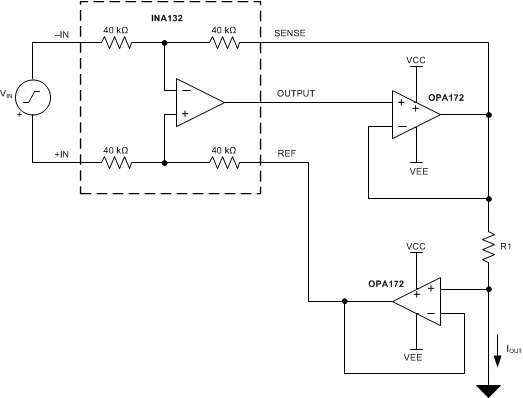
OPA172 OPA2172 OPA4172 ai_bidir_Isource_bos618.gifFigure 50. Bidirectional Current Source