SBOS223G December 2001 – August 2016 OPA690
PRODUCTION DATA.
- 1 Features
- 2 Applications
- 3 Description
- 4 Revision History
- 5 Device Comparison Table
- 6 Pin Configuration and Functions
- 7 Specifications
- 8 Detailed Description
- 9 Application and Implementation
- 10Power Supply Recommendations
- 11Layout
- 12Device and Documentation Support
- 13Mechanical, Packaging, and Orderable Information
Package Options
Mechanical Data (Package|Pins)
Thermal pad, mechanical data (Package|Pins)
Orderable Information
8 Detailed Description
8.1 Overview
The OPA690 provides an exceptional combination of high output power capability with a wideband, unity-gain stable voltage-feedback op amp using a new high slew rate input stage. The input stage provides a very high slew rate (1800 V/µs) while consuming relatively low quiescent current (5.5 mA). This exceptional full-power performance comes at the price of a slightly higher input noise voltage than alternative architectures.
The 5.5-nV/√Hz input voltage noise for the OPA690 is exceptionally low for this type of input stage.
8.2 Functional Block Diagram
8.3 Feature Description
8.3.1 Wideband Voltage-Feedback Operation
Typical differential input stages used for voltage feedback op amps are designed to steer a fixed-bias current to the compensation capacitor, setting a limit to the achievable slew rate. The OPA690 uses a new input stage which places the transconductance element between two input buffers, using their output currents as the forward signal.
Figure 36 shows the DC-coupled, gain of 2, dual power supply circuit configuration used as the basis of the ±5 V and Typical Characteristics: VS = ±5 V. For test purposes, the input impedance is set to 50 Ω with a resistor to ground and the output impedance is set to 50 Ω with a series output resistor. Voltage swings reported in the specifications are taken directly at the input and output pins, while output powers (dBm) are at the matched 50-Ω load. For the circuit of Figure 36, the total effective load is 100 Ω || 804 Ω. The disable control line is typically left open to ensure normal amplifier operation. Two optional components are included in Figure 36. An additional resistor (175 Ω) is included in series with the noninverting input. Combined with the 25-Ω DC source resistance looking back towards the signal generator, this gives an input bias current cancelling resistance that matches the 200-Ω source resistance seen at the inverting input (see DC Accuracy and Offset Control). In addition to the usual power-supply decoupling capacitors to ground, a 0.1-µF capacitor is included between the two power-supply pins. In practical printed-circuit board (PCB) layouts, this optional-added capacitor typically improves the 2nd-harmonic distortion performance by 3 dB to 6 dB.
Figure 37 shows the AC-coupled, gain of 2, single-supply circuit configuration which is the basis of the 5 V and Typical Characteristics: 5 V. Though not a rail-to-rail design, the OPA690 requires minimal input and output voltage headroom compared to other very wideband voltage-feedback op amps. It delivers a 3-VPP output swing on a single 5-V supply with > 150-MHz bandwidth. The key requirement of broadband single-supply operation is to maintain input and output signal swings within the useable voltage ranges at both the input and the output. The circuit of Figure 37 establishes an input midpoint bias using a simple resistive divider from the
5-V supply (two 698-Ω resistors). The input signal is then AC-coupled into the midpoint voltage bias. The input voltage can swing to within 1.5 V of either supply pin, giving a 2-VPP input signal range centered between the supply pins. The input impedance matching resistor (59 Ω) used for testing is adjusted to give a 50-Ω input load when the parallel combination of the biasing divider network is included.
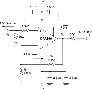 Figure 36. DC-Coupled, G = 2, Bipolar-Supply
Specification and Test Circuit
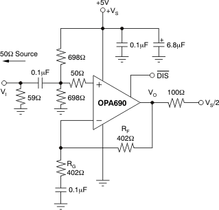 Figure 37. AC-Coupled, G = 2, Single-Supply
Specification and Test Circuit
Again, an additional resistor (50 Ω in this case) is included directly in series with the noninverting input. This minimum recommended value provides part of the dc source resistance matching for the noninverting input bias current. It is also used to form a simple parasitic pole to roll off the frequency response at very high frequencies
(> 500 MHz) using the input parasitic capacitance to form a bandlimiting pole. The gain resistor (RG) is AC-coupled, giving the circuit a DC gain of 1, which puts the input DC bias voltage (2.5 V) at the output as well. The output voltage can swing to within 1 V of either supply pin while delivering > 100-mA output current. A demanding 100-Ω load to a midpoint bias is used in this characterization circuit. The new output stage circuit used in the OPA690 can deliver large bipolar output currents into this midpoint load with minimal crossover distortion, as shown in the 5-V supply, 3rd-harmonic distortion plots.
8.3.2 Bandwidth Versus Gain: Noninverting Operation
Voltage-feedback op amps exhibit decreasing closed-loop bandwidth as the signal gain is increased. In theory, this relationship is described by the gain bandwidth product (GBP) shown in the Electrical Characteristics: VS = ±5 V. Ideally, dividing GBP by the noninverting signal gain (also called the Noise Gain, or NG) predicts the closed-loop bandwidth. In practice, this only holds true when the phase margin approaches 90°, as it does in high gain configurations. At low gains (increased feedback factors), most amplifiers exhibit a more complex response with lower phase margin. The OPA690 is compensated to give a slightly peaked response in a noninverting gain of 2 (see Figure 36). This results in a typical gain of 2 bandwidth of 220 MHz, far exceeding that predicted by dividing the 300 MHz GBP by 2. Increasing the gain causes the phase margin to approach 90° and the bandwidth to more closely approach the predicted value of (GBP/NG). At a gain of 10, the 30-MHz bandwidth shown in Electrical Characteristics: VS = ±5 V agrees with that predicted using the simple formula and the typical GBP of 300 MHz.
The frequency response in a gain of 2 may be modified to achieve exceptional flatness simply by increasing the noise gain to 2.5. One way to do this, without affecting the 2 signal gain, is to add an 804-Ω resistor across the two inputs in the circuit of Figure 36. A similar technique may be used to reduce peaking in unity-gain (voltage follower) applications. For example, by using a 402-Ω feedback resistor along with a 402-Ω resistor across the two op amp inputs, the voltage follower response is similar to the gain of 2 response of Figure 37. Reducing the value of the resistor across the op amp inputs further limits the frequency response due to increased noise gain.
The OPA690 exhibits minimal bandwidth reduction going to single-supply (5 V) operation as compared with ±5 V. This is because the internal bias control circuitry retains nearly constant quiescent current as the total supply voltage between the supply pins is changed.
8.3.3 Inverting Amplifier Operation
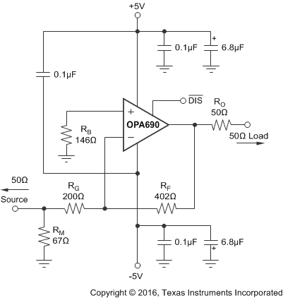
Because the OPA690 is a general-purpose, wideband voltage-feedback op amp, all of the familiar op amp application circuits are available to the designer. Inverting operation is one of the more common requirements and offers several performance benefits. Figure 38 shows a typical inverting configuration where the I/O impedances and signal gain from Figure 36 are retained in an inverting circuit configuration.
 Figure 38. Gain of –2 Example Circuit
In the inverting configuration, three key design considerations must be noted. The first is that the gain resistor (RG) becomes part of the signal channel input impedance. If input impedance matching is desired (which is beneficial whenever the signal is coupled through a cable, twisted-pair, long PCB trace, or other transmission line conductor), RG may be set equal to the required termination value and RF adjusted to give the desired gain. This is the simplest approach and results in optimum bandwidth and noise performance. However, at low inverting gains, the resultant feedback resistor value can present a significant load to the amplifier output. For an inverting gain of 2, setting RG to 50 Ω for input matching eliminates the requirement for RM but requires a 100-Ω feedback resistor. This has the interesting advantage that the noise gain becomes equal to 2 for a 50-Ω source impedance—the same as the noninverting circuits considered in the previous section. The amplifier output, however, now sees the 100-Ω feedback resistor in parallel with the external load. In general, the feedback resistor must be limited to the 200-Ω to 1.5-kΩ range. In this case, it is preferable to increase both the RF and RG values, as shown in Figure 38, and then achieve the input matching impedance with a third resistor (RM) to ground. The total input impedance becomes the parallel combination of RG and RM.
The second major consideration, touched on in the previous paragraph, is that the signal source impedance becomes part of the noise gain equation and influences the bandwidth. For the example in Figure 38, the RM value combines in parallel with the external 50-Ω source impedance, yielding an effective driving impedance of 50 Ω || 67 Ω = 28.6 Ω. This impedance is added in series with RG for calculating the noise gain (NG). The resultant NG is 2.8 for Figure 38, as opposed to only 2 if RM could be eliminated as discussed above. Therefore, the bandwidth is slightly lower for the gain of ±2 circuit of Figure 38 than for the gain of 2 circuit of Figure 36.
The third important consideration in inverting amplifier design is setting the bias current cancellation resistor on the noninverting input (RB). If this resistor is set equal to the total DC resistance looking out of the inverting node, the output DC error, due to the input bias currents, is reduced to (Input Offset Current) × RF. If the 50-Ω source impedance is DC-coupled in Figure 38, the total resistance to ground on the inverting input is 228 Ω. Combining this in parallel with the feedback resistor gives the RB = 146 Ω used in this example. To reduce the additional high-frequency noise introduced by this resistor, it is sometimes bypassed with a capacitor. As long as RB < 350 Ω, the capacitor is not required because the total noise contribution of all other terms is less than that of the op amp input noise voltage. As a minimum, the OPA690 requires an RB value of 50 Ω to damp out parasitic-induced peaking which is a direct short to ground on the noninverting input runs the risk of a very high-frequency instability in the input stage.
8.3.4 Output Current and Voltage
The OPA690 provides output voltage and current capabilities that are unsurpassed in a low-cost monolithic op amp. Under no-load conditions at 25°C, the output voltage typically swings closer than 1 V to either supply rail; the specified swing limit is within 1.2 V of either rail. Into a 15-Ω load (the minimum tested load), it delivers more than ±160 mA.
The specifications described previously, though familiar in the industry, consider voltage and current limits separately. In many applications, it is the voltage × current, or V-I product, which is more relevant to circuit operation. Refer to Figure 19, the Output Voltage and Current Limitations plot in Typical Characteristics: VS = ±5 V. The X- and Y-axes of this graph show the zero-voltage output current limit and the zero-current output voltage limit, respectively. The four quadrants give a more detailed view of the OPA690 output drive capabilities, noting that the graph is bounded by a safe operating area of 1-W maximum internal power dissipation. Superimposing resistor load lines onto the plot shows that the OPA690 can drive ±2.5 V into 25 Ω or ±3.5 V into 50 Ω without exceeding the output capabilities or the 1-W dissipation limit. A 100-Ω load line (the standard test circuit load) shows the full ±3.9-V output swing capability, as shown in Typical Characteristics: VS = ±5 V.
The minimum specified output voltage and current specifications over temperature are set by worst-case simulations at the cold temperature extreme. Only at cold startup will the output current and voltage decrease to the numbers shown in Electrical Characteristics: VS = ±5 V. As the output transistors deliver power, their junction temperatures increase, decreasing their VBEs (increasing the available output voltage swing) and increasing their current gains (increasing the available output current). In steady-state operation, the available output voltage and current is always greater than that shown in the overtemperature specifications because the output stage junction temperatures is higher than the minimum specified operating ambient.
To protect the output stage from accidental shorts to ground and the power supplies, output short-circuit protection is included in the OPA690. The circuit acts to limit the maximum source or sink current to approximately 250 mA.
8.3.5 Driving Capacitive Loads
One of the most demanding and yet very common load conditions for an op amp is capacitive loading. Often, the capacitive load is the input of an ADC—including additional external capacitance which may be recommended to improve ADC linearity. A high-speed, high open-loop gain amplifier like the OPA690 can be very susceptible to decreased stability and closed-loop response peaking when a capacitive load is placed directly on the output pin. When the amplifier's open-loop output resistance is considered, this capacitive load introduces an additional pole in the signal path that can decrease the phase margin. Several external solutions to this problem have been suggested. When the primary considerations are frequency response flatness, pulse response fidelity, and distortion, the simplest and most effective solution is to isolate the capacitive load from the feedback loop by inserting a series-isolation resistor between the amplifier output and the capacitive load. This does not eliminate the pole from the loop response, but rather shifts it and adds a zero at a higher frequency. The additional zero acts to cancel the phase lag from the capacitive load pole, thus increasing the phase margin and improving stability.
The typical characteristics show the recommended RS versus capacitive load (Figure 15 for ±5 V and Figure 30 for 5 V) and the resulting frequency response at the load. Parasitic capacitive loads greater than 2 pF can begin to degrade the performance of the OPA690. Long PCB traces, unmatched cables, and connections to multiple devices can easily exceed this value. Always consider this effect carefully, and add the recommended series resistor as close as possible to the OPA690 output pin (see Layout Guidelines).
The criterion for setting this RS resistor is a maximum bandwidth, flat frequency response at the load. For the OPA690 operating in a gain of 2, the frequency response at the output pin is already slightly peaked without the capacitive load requiring relatively high values of RS to flatten the response at the load. Increasing the noise gain reduces the peaking as described previously. The circuit of Figure 39 demonstrates this technique, allowing lower values of RS to be used for a given capacitive load.
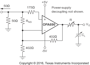 Figure 39. Capacitive Load Driving With Noise Gain Tuning
This gain of 2 circuit includes a noise gain tuning resistor across the two inputs to increase the noise gain, increasing the unloaded phase margin for the op amp. Although this technique reduces the required RS resistor for a given capacitive load, it does increase the noise at the output. It also decreases the loop gain, slightly decreasing the distortion performance. If, however, the dominant distortion mechanism arises from a high RS value, significant dynamic range improvement can be achieved using this technique. Figure 40 shows the required RS versus CLOAD parametric on noise gain using this technique. This is the circuit of Figure 39 with RNG adjusted to increase the noise gain (increasing the phase margin) then sweeping CLOAD and finding the required RS to get a flat frequency response. This plot also gives the required RS versus CLOAD for the OPA690 operated at higher signal gains.
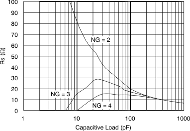 Figure 40. Required RS vs Noise Gain
8.3.6 Distortion Performance
The OPA690 provides good distortion performance into a 100-Ω load on ±5-V supplies. Relative to alternative solutions, it provides exceptional performance into lighter loads and/or operating on a single 5-V supply. Generally, until the fundamental signal reaches very high frequency or power levels, the 2nd-harmonic dominates the distortion with a negligible 3rd-harmonic component. Focusing then on the 2nd-harmonic, increasing the load impedance improves distortion directly. Remember that the total load includes the feedback network; in the noninverting configuration (see Figure 36), this is sum of RF + RG, while in the inverting configuration it is just RF. Also, providing an additional supply-decoupling capacitor (0.1 µF) between the supply pins (for bipolar operation) improves the 2nd-order distortion slightly (3 dB to 6 dB).
In most op amps, increasing the output voltage swing increases harmonic distortion directly. The new output stage used in the OPA690 actually holds the difference between fundamental power and the 2nd- and 3rd-harmonic powers relatively constant with increasing output power until very large output swings are required
(> 4 VPP). This also shows up in the 2-tone, 3rd-order intermodulation spurious (IM3) response curves. The 3rd-order spurious levels are moderately low at low output power levels. The output stage continues to hold them low even as the fundamental power reaches very high levels. As the Typical Characteristics: VS = ±5 V show, the spurious intermodulation powers do not increase as predicted by a traditional intercept model. As the fundamental power level increases, the dynamic range does not decrease significantly. For two tones centered at 20 MHz, with 10 dBm/tone into a matched 50-Ω load (that is, 2 VPP for each tone at the load, which requires 8 VPP for the overall two-tone envelope at the output pin), Figure 14 shows 47-dBc difference between the test tone powers and the 3rd-order intermodulation spurious powers. This performance improves further when operating at lower frequencies.
8.3.7 Noise Performance
High slew rate, unity-gain stable, voltage-feedback op amps usually achieve their slew rate at the expense of a higher input noise voltage. The 5.5-nV/√Hz input voltage noise for the OPA690 is, however, much lower than comparable amplifiers. The input-referred voltage noise, and the two input-referred current noise terms, combine to give low output noise under a wide variety of operating conditions. Figure 41 shows the op amp noise analysis model with all the noise terms included. In this model, all noise terms are taken to be noise voltage or current density terms in either nV/√Hz or pA/√Hz.
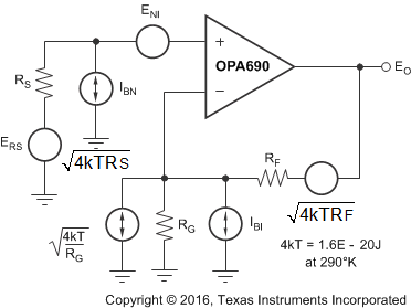 Figure 41. Op Amp Noise Analysis Model
The total output spot noise voltage can be computed as the square root of the sum of all squared output noise voltage contributors. Equation 1 shows the general form for the output noise voltage using the terms shown in Figure 41.

Dividing this expression by the noise gain [NG = (1 + RF/RG)] gives the equivalent input-referred spot noise voltage at the noninverting input, as shown in Equation 2.

Evaluating these two equations for the OPA690 circuit and component values (see Figure 36) gives a total output spot noise voltage of 12.3 nV/√Hz and a total equivalent input spot noise voltage of 6.1 nV/√Hz. This is including the noise added by the bias current cancellation resistor (175 Ω) on the noninverting input. This total input-referred spot noise voltage is only slightly higher than the 5.5-nV/√Hz specification for the op amp voltage noise alone. This is the case as long as the impedances appearing at each op amp input are limited to the previously recommend maximum value of 300 Ω. Keeping both (RF || RG) and the noninverting input source impedance less than 300 Ω satisfies both noise and frequency response flatness considerations. Because the resistor-induced noise is relatively negligible, additional capacitive decoupling across the bias current cancellation resistor (RB) for the inverting op amp configuration of Figure 38 is not required.
8.3.8 DC Accuracy and Offset Control
The balanced input stage of a wideband voltage-feedback op amp allows good output DC accuracy in a wide variety of applications. The power-supply current trim for the OPA690 gives even tighter control than comparable amplifiers. Although the high-speed input stage does require relatively high input bias current (typically ±8 µA at each input terminal), the close matching between them may be used to reduce the output DC error caused by this current. The total output offset voltage may be considerably reduced by matching the DC source resistances appearing at the two inputs. This reduces the output dc error due to the input bias currents to the offset current times the feedback resistor. Evaluating the configuration of Figure 36, and using worst-case 25°C input offset voltage and current specifications, gives a worst-case output offset voltage equal to:
–(NG = noninverting signal gain)
±(NG × VOS(MAX)) ± (RF × IOS(MAX))
= ±(2 × 4 mV) ± (402 Ω × 1 µA)
= ±8.4 mV
A fine-scale output offset null, or DC operating point adjustment, is often required. Numerous techniques are available for introducing DC offset control into an op amp circuit. Most of these techniques eventually reduce to adding a DC current through the feedback resistor. In selecting an offset trim method, one key consideration is the impact on the desired signal path frequency response. If the signal path is intended to be noninverting, the offset control is best applied as an inverting summing signal to avoid interaction with the signal source. If the signal path is intended to be inverting, applying the offset control to the noninverting input may be considered. However, the DC offset voltage on the summing junction sets up a DC current back into the source that must be considered. Applying an offset adjustment to the inverting op amp input can change the noise gain and frequency response flatness. For a DC-coupled inverting amplifier, see Figure 42 for one example of an offset adjustment technique that has minimal impact on the signal frequency response. In this case, the DC offsetting current is brought into the inverting input node through resistor values that are much larger than the signal path resistors. This ensures that the adjustment circuit has minimal effect on the loop gain and hence, the frequency response.
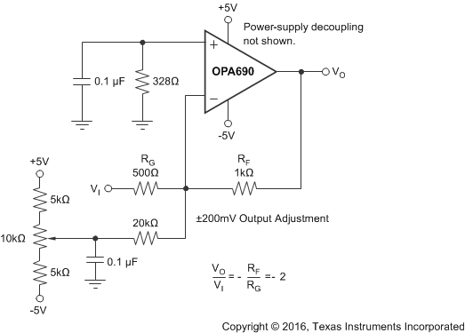 Figure 42. DC-Coupled, Inverting Gain of –2, With Offset Adjustment
8.4 Device Functional Modes
8.4.1 Disable Operation
The OPA690 provides an optional disable feature that may be used either to reduce system power or to implement a simple channel multiplexing operation. If the DIS control pin is left unconnected, the OPA690 operates normally. To disable, the control pin must be asserted LOW. Figure 43 shows a simplified internal circuit for the disable control feature.
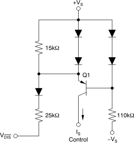 Figure 43. Simplified Disable Control Circuit
In normal operation, base current to Q1 is provided through the 110-kΩ resistor, while the emitter current through the 15-kΩ resistor sets up a voltage drop that is inadequate to turn on the two diodes in Q1's emitter. As VDIS is pulled LOW, additional current is pulled through the 15-kΩ resistor, eventually turning on those two diodes (approximately 75 µA). At this point, any further current pulled out of VDIS goes through those diodes holding the emitter-base voltage of Q1 at approximately 0 V. This shuts off the collector current out of Q1, turning the amplifier off. The supply current in the disable mode are only those required to operate the circuit of Figure 43. Additional circuitry ensures that turnon time occurs faster than turnoff time (make-before-break).
When disabled, the output and input nodes go to a high-impedance state. If the OPA690 is operating at a gain of 1, this shows a very high impedance at the output and exceptional signal isolation. If operating at a gain greater than 1, the total feedback network resistance (RF + RG) appears as the impedance looking back into the output, but the circuit still shows very high forward and reverse isolation. If configured as an inverting amplifier, the input and output is connected through the feedback network resistance (RF + RG) and the isolation is very poor as a result.
One key parameter in disable operation is the output glitch when switching in and out of the disabled mode. Figure 44 shows these glitches for the circuit of Figure 36 with the input signal at 0 V. The glitch waveform at the output pin is plotted along with the DIS pin voltage.
The transition edge rate (dV/dt) of the DIS control line influences this glitch. For the plot of Figure 44, the edge rate was reduced until no further reduction in glitch amplitude was observed. This approximately 1-V/ns maximum slew rate may be achieved by adding a simple RC filter into the DIS pin from a higher speed logic line. If extremely fast transition logic is used, a 1-kΩ series resistor between the logic gate and the DIS input pin provides adequate bandlimiting using just the parasitic input capacitance on the DIS pin while still ensuring adequate logic level swing.
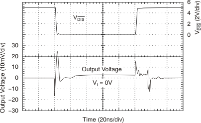 Figure 44. Disable or Enable Glitch