SBOS867C August 2017 – October 2023 OPA838
PRODUCTION DATA
- 1
- 1 Features
- 2 Applications
- 3 Description
- 4 Revision History
- 5 Device Comparison Table
- 6 Pin Configuration and Functions
-
7 Specifications
- 7.1 Absolute Maximum Ratings
- 7.2 ESD Ratings
- 7.3 Recommended Operating Conditions
- 7.4 Thermal Information
- 7.5 Electrical Characteristics: VS = 5 V
- 7.6 Electrical Characteristics: VS = 3 V
- 7.7 Typical Characteristics: VS = 5 V
- 7.8 Typical Characteristics: VS = 3 V
- 7.9 Typical Characteristics: Over Supply Range
- 8 Detailed Description
- 9 Application and Implementation
- 10Device and Documentation Support
- Mechanical, Packaging, and Orderable Information
Package Options
Mechanical Data (Package|Pins)
Thermal pad, mechanical data (Package|Pins)
Orderable Information
9.1.1 Noninverting Amplifier
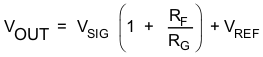
The OPA838 can be used as noninverting amplifier with signal input to the noninverting input (VIN+). Figure 8-1 illustrates a basic block diagram of the circuit. VREF is often ground when split supplies are used.
If VIN = VREF + VSIG, and the gain setting resistor (RG) is dc referenced to VREF, use Equation 1 to calculate the output of the amplifier.
The noninverting signal gain (also called the
noise gain) of the circuit is set by: 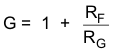
VREF provides a reference around which the input and output signals swing. Output signals are in-phase with the input signals within the flat portion of the frequency response. For a high-speed, low-noise device like the OPA838, the values selected for RF (and the RG for the desired gain) can strongly influence the operation of the circuit. For the characteristic curves, the noninverting circuit of Figure 9-1 shows the test configuration. Table 9-1 lists the recommended resistor values over gain.
 Figure 9-1 Noninverting Characterization Circuit
Table 9-1 lists the recommended resistor values from target gains of 6 V/V to 20 V/V. This table controls the RF and RG values to set the resistor noise contribution at approximately 40% of the total output noise power. This increases the spot noise at the output over what the op amp voltage noise produces by 20%. Lower values reduce the output noise of any design at the cost of more power in the feedback circuit. Using the TINA model and simulation tool shows the impact of different resistor value choices on response shape and noise.
| TARGET AVERAGE | RF (Ω) | RG (Ω) | ACTUAL GAIN (V/V) | GAIN (dB) |
|---|---|---|---|---|
| 6 | 1000 | 200 | 6 | 15.56 |
| 7 | 1180 | 196 | 7.02 | 16.93 |
| 8 | 1370 | 196 | 7.99 | 18.05 |
| 9 | 1540 | 191 | 9.06 | 19.15 |
| 10 | 1690 | 187 | 10.04 | 20.03 |
| 11 | 1870 | 187 | 11 | 20.83 |
| 12 | 2050 | 187 | 11.96 | 21.56 |
| 13 | 2210 | 182 | 13.14 | 22.37 |
| 14 | 2370 | 182 | 14.02 | 22.94 |
| 15 | 2550 | 182 | 15.01 | 23.53 |
| 16 | 2740 | 182 | 16.05 | 24.11 |
| 17 | 2870 | 178 | 17.12 | 24.67 |
| 18 | 3090 | 182 | 17.98 | 25.09 |
| 19 | 3240 | 178 | 19.20 | 25.67 |
| 20 | 3400 | 178 | 20.1 | 26.06 |
| 21 | 3570 | 178 | 21.06 | 26.47 |