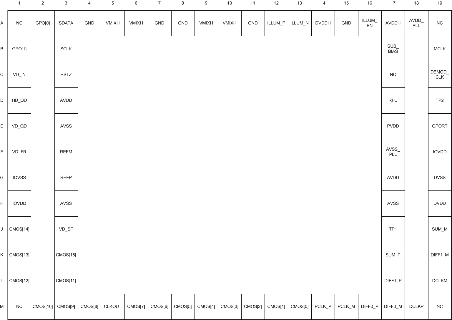
| AVDD |
D3, G17 |
Power |
— |
1.8-V analog VDD |
| AVDD_PLL |
A18 |
Power |
— |
1.8-V PLL VDD |
| AVDDH |
A17 |
Power |
— |
3.3-V analog VDD |
| AVSS |
E3, H3, H17 |
GND |
— |
Analog ground |
| AVSS_PLL |
F17 |
GND |
— |
PLL GND |
| CLKOUT |
M5 |
O |
IOVDD |
Parallel data clock output |
| CMOS[0] |
M13 |
O |
IOVDD |
Parallel data output bit 0 |
| CMOS[1] |
M12 |
O |
IOVDD |
Parallel data output bit 1 |
| CMOS[2] |
M11 |
O |
IOVDD |
Parallel data output bit 2 |
| CMOS[3] |
M10 |
O |
IOVDD |
Parallel data output bit 3 |
| CMOS[4] |
M9 |
O |
IOVDD |
Parallel data output bit 4 |
| CMOS[5] |
M8 |
O |
IOVDD |
Parallel data output bit 5 |
| CMOS[6] |
M7 |
O |
IOVDD |
Parallel data output bit 6 |
| CMOS[7] |
M6 |
O |
IOVDD |
Parallel data output bit 7 |
| CMOS[8] |
M4 |
O |
IOVDD |
Parallel data output bit 8 |
| CMOS[9] |
M3 |
O |
IOVDD |
Parallel data output bit 9 |
| CMOS[10] |
M2 |
O |
IOVDD |
Parallel data output bit 10 |
| CMOS[11] |
L3 |
O |
IOVDD |
Parallel data output bit 11 |
| CMOS[12] |
L1 |
O |
IOVDD |
Parallel data output bit 12 |
| CMOS[13] |
K1 |
O |
IOVDD |
Parallel data output bit 13 |
| CMOS[14] |
J1 |
O |
IOVDD |
Parallel data output bit 14 |
| CMOS[15] |
K3 |
O |
IOVDD |
Parallel data output bit 15 |
| DCLKM |
L19 |
O |
LVDS |
Negative LVDS bit clock |
| DCLKP |
M18 |
O |
LVDS |
Positive LVDS bit clock |
| DEMOD_CLK |
C19 |
I |
IOVDD |
Demodulation clock input (optional).
This pin has a weak internal pulldown resistor. |
| DIFF0_M |
M17 |
O |
LVDS |
Negative LVDS DIFF0 data pin |
| DIFF0_P |
M16 |
O |
LVDS |
Positive LVDS DIFF0 data pin |
| DIFF1_M |
K19 |
O |
LVDS |
Negative LVDS DIFF1 data pin |
| DIFF1_P |
L17 |
O |
LVDS |
Positive LVDS DIFF1 data pin |
| DVDD |
H19 |
Power |
— |
1.8-V digital VDD |
| DVDDH |
A14 |
Power |
— |
3.3-V digital VDD |
| DVSS |
G19 |
GND |
— |
Digital GND |
| GND |
A4, A7, A8, A11, A15 |
GND |
— |
Ground |
| GPO[0] |
A2 |
O |
IOVDD |
General-purpose output |
| GPO[1] |
B1 |
O |
IOVDD |
General-purpose output |
| HD_QD |
D1 |
O |
IOVDD |
Quad-frame line sync output |
| ILLUM_EN |
A16 |
O |
DVDDH |
Illumination enable |
| ILLUM_N |
A13 |
O |
DVDDH |
Illumination modulation signal; active low |
| ILLUM_P |
A12 |
O |
DVDDH |
Illumination modulation signal; active high |
| IOVDD |
H1, F19 |
Power |
— |
1.8-V to 3.3-V IOVDD |
| IOVSS |
G1 |
GND |
— |
I/O GND |
| MCLK |
B19 |
I |
IOVDD |
Main clock input for TG.
This pin has a weak internal pulldown resistor. |
| NC |
A1, A19, C17, M1, M19 |
NC |
— |
No connection |
| PCLK_M |
M15 |
O |
LVDS |
Negative LVDS pixel clock |
| PCLK_P |
M14 |
O |
LVDS |
Positive LVDS pixel clock |
| PVDD |
E17 |
Power |
— |
3.3-V pixel VDD |
| QPORT |
E19 |
I/O |
IOVDD |
Debug port.
Pullup with an external 1-kΩ resistor to IOVDD instead. |
| REFM |
F3 |
Analog In |
— |
Connect REFM to GND |
| REFP |
G3 |
Analog Out |
— |
ADC reference; connect a 10-nF capacitor close to REFM and REFP. |
| RFU |
D17 |
RFU |
— |
Reserved for future use |
| RSTZ |
C3 |
I |
IOVDD |
Sensor reset input. This pin has a weak internal pullup resistor. |
| SCL |
B3 |
I |
IOVDD |
Clock I2C slave interface |
| SDATA |
A3 |
I/O |
IOVDD |
Data I2C slave interface |
| SUB_BIAS |
B17 |
Power |
— |
Substrate bias |
| SUM_M |
J19 |
O |
LVDS |
Negative LVDS sum data |
| SUM_P |
K17 |
O |
LVDS |
Positive LVDS sum data |
| TP1 |
J17 |
O |
— |
Debug pin 1, connect to a test pad on the board |
| TP2 |
D19 |
O |
— |
Debug pin 2, connect to a test pad on the board |
| VD_FR |
F1 |
O |
IOVDD |
Frame sync output |
| VD_IN |
C1 |
I |
IOVDD |
Frame sync input (optional) |
| VD_QD |
E1 |
O |
IOVDD |
Quad-frame sync output |
| VD_SF |
J3 |
O |
— |
Sub-frame sync output |
| VMIXH |
A5, A6, A9, A10 |
Power |
— |
Mix driver power |
