SBFS038A June 2012 – September 2015 PCM2903C
PRODUCTION DATA.
- 1 Features
- 2 Applications
- 3 Description
- 4 Revision History
- 5 Device Comparison Table
- 6 Pin Configuration and Functions
-
7 Specifications
- 7.1 Absolute Maximum Ratings
- 7.2 ESD Ratings
- 7.3 Recommended Operating Conditions
- 7.4 Thermal Information
- 7.5 Electrical Characteristics
- 7.6
Typical Characteristics
- 7.6.1 Typical Characteristics: ADC
- 7.6.2 Typical Characteristics: DAC
- 7.6.3 Typical Characteristics: ADC Output Spectrum
- 7.6.4 Typical Characteristics: DAC Output Spectrum
- 7.6.5 Typical Characteristics: Supply Current
- 7.6.6 Typical Characteristics: ADC Digital Decimation Filter Frequency Response
- 7.6.7 Typical Characteristics: ADC Digital High-Pass Filter Frequency Response
- 7.6.8 Typical Characteristics: ADC Analog Antialiasing Filter Frequency Response
- 7.6.9 Typical Characteristics: DAC Digital Interpolation Filter Frequency Response
- 7.6.10 Typical Characteristics: DAC Analog Fir Filter Frequency Response
- 7.6.11 Typical Characteristics: DAC Analog Low-Pass Filter Frequency Response
- 8 Parameter Measurement Information
- 9 Detailed Description
- 10Application and Implementation
- 11Power Supply Recommendations
- 12Layout
- 13Device and Documentation Support
- 14Mechanical, Packaging, and Orderable Information
Package Options
Mechanical Data (Package|Pins)
- DB|28
Thermal pad, mechanical data (Package|Pins)
Orderable Information
10 Application and Implementation
NOTE
Information in the following applications sections is not part of the TI component specification, and TI does not warrant its accuracy or completeness. TI’s customers are responsible for determining suitability of components for their purposes. Customers should validate and test their design implementation to confirm system functionality.
10.1 Application Information
The VBUS allows the device to know when it has been plugged to a USB connection port. The SSPND’ flag will notify when the USB input is idle for at least 5ms; this flag can be used to control or notify subsequent circuits. More functional details can be found on Interface Sequence.
10.2 Typical Application
Figure 41 illustrates a typical circuit connection for a simple application. The circuit illustrated is for information only. The entire board design should be considered to meet the USB specification as a USB-compliant product.
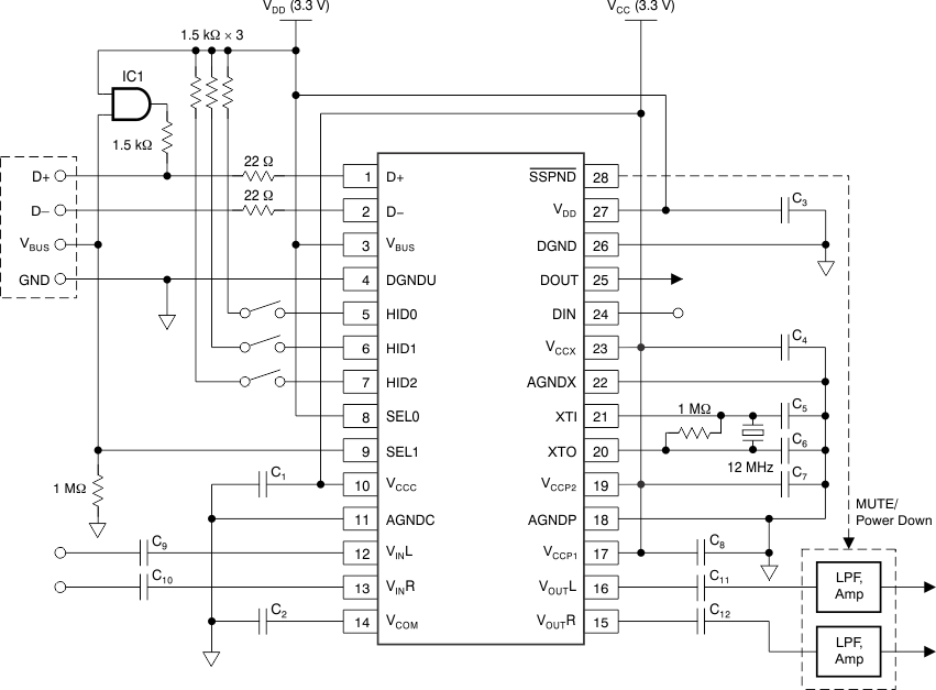
NOTE:
IC1 must be driven by VDD with a 5-V tolerant input.
C1, C2, C3, C4, C7, C8: 10 μF
C5, C6: 10 pF to 33 pF (depending on crystal resonator)
C9, C10, C11, C12: The capacitance may vary depending on design.
10.2.1 Design Requirements
For this example, Table 6 lists the design parameters.
Table 6. Design Parameters
| DESIGN PARAMETER | EXAMPLE VALUE | |||
|---|---|---|---|---|
| Input voltage range | 3 V to 3.6 V | |||
| Current | 50 mA to 70 mA | |||
| Input clock frequency | 11.994 MHz to 12.006 MHz | |||
10.2.2 Detailed Design Procedure
The PCM2903C is a simple design device since it is capable to connect directly to a USB port. Only two external ICs are needed, a 3.3-V regulator and an AND Gate. The switches connected to the HID ports must be normally open. Other than this, it only needs decoupling capacitors on the voltage source pins.
10.2.3 Application Curves
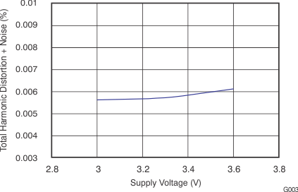 Figure 42. ADC Total Harmonic Distortion + Noise at –1 dB vs Supply Voltage
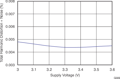 Figure 44. DAC Total Harmonic Distortion + Noise at 0 dB vs Supply Voltage
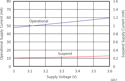 Figure 46. Operational and Suspend Supply Current vs Supply Voltage
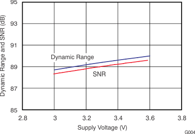 Figure 43. ADC Dynamic Range and SNR vs Supply Voltage
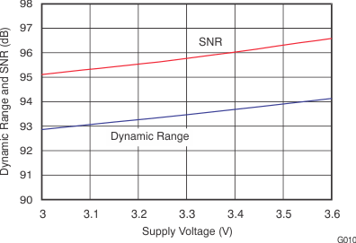 Figure 45. DAC Dynamic Range and SNR vs Supply Voltage
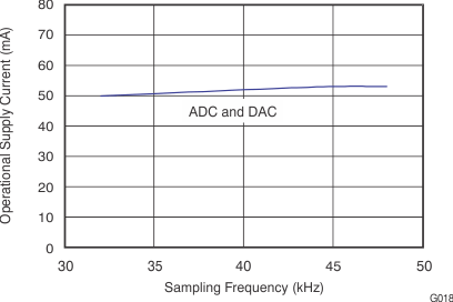 Figure 47. Operational Supply Current vs Sampling Frequency