SGUS033A February 2002 – May 2016 SMJ320C6203
PRODUCTION DATA.
- 1 Features
- 2 Description
- 3 Revision History
- 4 Description (continued)
- 5 Characteristics of the C6203 DSP
- 6 Pin Configuration and Functions
-
7 Specifications
- 7.1 Absolute Maximum Ratings
- 7.2 Recommended Operating Conditions
- 7.3 Thermal Information
- 7.4 Electrical Characteristics
- 7.5 Timing Requirements for CLKIN (PLL Used)
- 7.6 Timing Requirements for CLKIN [PLL Bypassed (x1)]
- 7.7 Timing Requirements for XCLKIN
- 7.8 Timing Requirements for Asynchronous Memory Cycles
- 7.9 Timing Requirements for Synchronous-Burst SRAM Cycles
- 7.10 Timing Requirements for Synchronous DRAM Cycles
- 7.11 Timing Requirements for the HOLD/HOLDA Cycles
- 7.12 Timing Requirements for Reset
- 7.13 Timing Requirements for Interrupt Response Cycles
- 7.14 Timing Requirements for Synchronous FIFO Interface
- 7.15 Timing Requirements for Asynchronous Peripheral Cycles
- 7.16 Timing Requirements With External Device as Bus Master
- 7.17 Timing Requirements With C62x as Bus Master
- 7.18 Timing Requirements With External Device as Asynchronous Bus Master
- 7.19 Timing Requirements for Expansion Bus Arbitration (Internal Arbiter Enabled)
- 7.20 Timing Requirements for McBSP
- 7.21 Timing Requirements for FSR when GSYNC = 1
- 7.22 Timing Requirements for McBSP as SPI Master or Slave: CLKSTP = 10b, CLKXP = 0
- 7.23 Timing Requirements for McBSP as SPI Master or Slave: CLKSTP = 11b, CLKXP = 0
- 7.24 Timing Requirements for McBSP as SPI Master or Slave: CLKSTP = 10b, CLKXP = 1
- 7.25 Timing Requirements for McBSP as SPI Master or Slave: CLKSTP = 11b, CLKXP = 1
- 7.26 Timing Requirements for Timer Inputs
- 7.27 Timing Requirements for JTAG Test Port
- 7.28 Switching Characteristics for CLKOUT2
- 7.29 Switching Characteristics for XFCLK
- 7.30 Asynchronous Memory Timing Switching Characteristics
- 7.31 Switching Characteristics for Synchronous-Burst SRAM Cycles
- 7.32 Switching Characteristics for Synchronous DRAM Cycles
- 7.33 Switching Characteristics for the HOLD/HOLDA Cycles
- 7.34 Switching Characteristics for Reset
- 7.35 Switching Characteristics for Interrupt Response Cycles
- 7.36 Switching Characteristics for Synchronous FIFO Interface
- 7.37 Switching Characteristics for Asynchronous Peripheral Cycles
- 7.38 Switching Characteristics With External Device as Bus Master
- 7.39 Switching Characteristics With C62x as Bus Master
- 7.40 Switching Characteristics With External Device as Asynchronous Bus Master
- 7.41 Switching Characteristics for Expansion Bus Arbitration (Internal Arbiter Enabled)
- 7.42 Switching Characteristics for Expansion Bus Arbitration (Internal Arbiter Disabled)
- 7.43 Switching Characteristics for McBSP
- 7.44 Switching Characteristics for McBSP as SPI Master or Slave
- 7.45 Switching Characteristics for McBSP as SPI Master or Slave: CLKSTP = 11b, CLKXP = 0
- 7.46 Switching Characteristics for McBSP as SPI Master or Slave: CLKSTP = 10b, CLKXP = 1
- 7.47 Switching Characteristics for McBSP as SPI Master or Slave: CLKSTP = 11b, CLKXP = 1
- 7.48 Switching Characteristics for DMAC Outputs
- 7.49 Switching Characteristics for Timer Outputs
- 7.50 Switching Characteristics for Power-Down Outputs
- 7.51 Switching Characteristics for JTAG Test Port
- 8 Parameter Measurement Information
- 9 Detailed Description
- 10Application and Implementation
- 11Power Supply Recommendations
- 12Device and Documentation Support
- 13Mechanical, Packaging, and Orderable Information
Package Options
Refer to the PDF data sheet for device specific package drawings
Mechanical Data (Package|Pins)
- GLP|429
Thermal pad, mechanical data (Package|Pins)
Orderable Information
9 Detailed Description
9.1 Functional Block Diagram
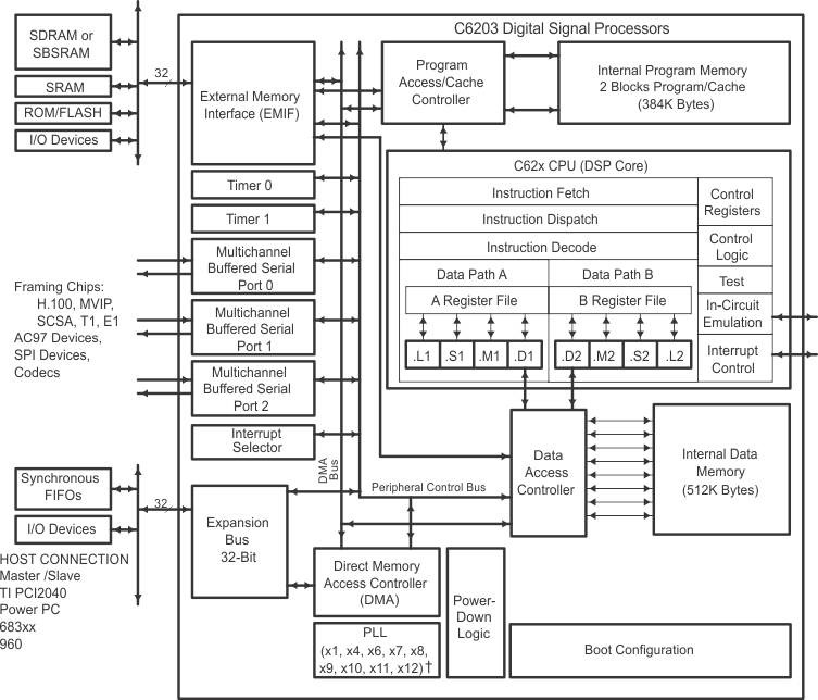
9.2 Feature Description
9.2.1 Signal Groups Description
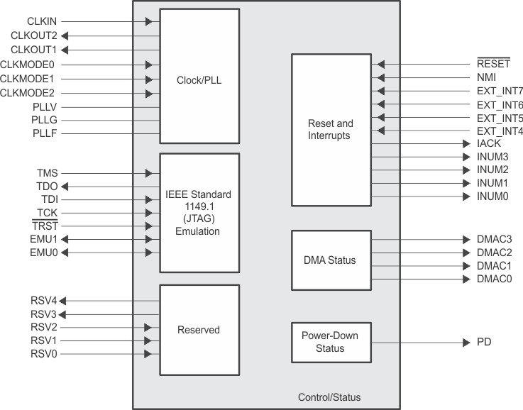 Figure 50. CPU (DSP Core) Signals
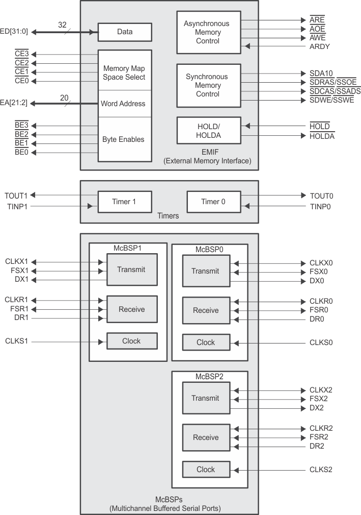 Figure 51. Peripheral Signals
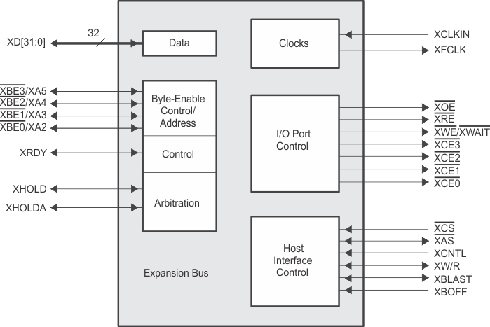 Figure 52. Peripheral Signals (continued)
9.2.2 CPU (DSP Core) Description
The CPU fetches VelociTI advanced VLIW (256 bits wide) to supply up to eight 32-bit instructions to the eight functional units during every clock cycle. The VelociTI VLIW architecture features controls by which all eight units do not have to be supplied with instructions if they are not ready to execute. The first bit of every 32-bit instruction determines if the next instruction belongs to the same execute packet as the previous instruction, or whether it should be executed in the following clock as a part of the next execute packet. Fetch packets are always 256 bits wide; however, the execute packets can vary in size. The variable-length execute packets are a key memory-saving feature, distinguishing the C62x CPU from other VLIW architectures.
The CPU features two sets of functional units. Each set contains four units and a register file. One set contains functional units .L1, .S1, .M1, and .D1; the other set contains units .D2, .M2, .S2, and .L2. The two register files each contain 16 32-bit registers for a total of 32 general-purpose registers. The two sets of functional units, along with two register files, compose sides A and B of the CPU (see Functional Block Diagram and Figure 53). The four functional units on each side of the CPU can freely share the 16 registers belonging to that side. Additionally, each side features a single data bus connected to all the registers on the other side, by which the two sets of functional units can access data from the register files on the opposite side. Register access by functional units on the same side of the CPU as the register file can service all the units in a single clock cycle. Register access using the register file across the CPU supports one read and one write per cycle.
Another key feature of the C62x CPU is the load/store architecture, where all instructions operate on registers (as opposed to data in memory). Two sets of data-addressing units (.D1 and .D2) are responsible for all data transfers between the register files and the memory. The data address driven by the .D units allows data addresses generated from one register file to be used to load or store data to or from the other register file. The C62x CPU supports a variety of indirect addressing modes using either linear- or circular-addressing modes with 5- or 15-bit offsets. All instructions are conditional, and most instructions can access any of the 32 registers. However, some registers are singled out to support specific addressing or to hold the condition for conditional instructions (if the condition is not automatically true). The two .M functional units are dedicated for multiplies. The two .S and .L functional units perform a general set of arithmetic, logical, and branch functions with results available every clock cycle.
The processing flow begins when a 256-bit-wide instruction fetch packet is fetched from a program memory. The 32-bit instructions destined for the individual functional units are linked together by 1 bits in the least significant bit (LSB) position of the instructions. The instructions that are chained together for simultaneous execution (up to eight in total) compose an execute packet. A 0 in the LSB of an instruction breaks the chain, effectively placing the instructions that follow it in the next execute packet. If an execute packet crosses the 256-bit-wide fetch-packet boundary, the assembler places it in the next fetch packet, while the remainder of the current fetch packet is padded with NOP instructions. The number of execute packets within a fetch packet can vary from one to eight. Execute packets are dispatched to their respective functional units at the rate of one per clock cycle and the next 256-bit fetch packet is not fetched until all the execute packets from the current fetch packet have been dispatched. After decoding, the instructions simultaneously drive all active functional units for a maximum execution rate of eight instructions every clock cycle. While most results are stored in 32-bit registers, they can be subsequently moved to memory as bytes or half-words as well. All load and store instructions are byte-, half-word, or word-addressable.
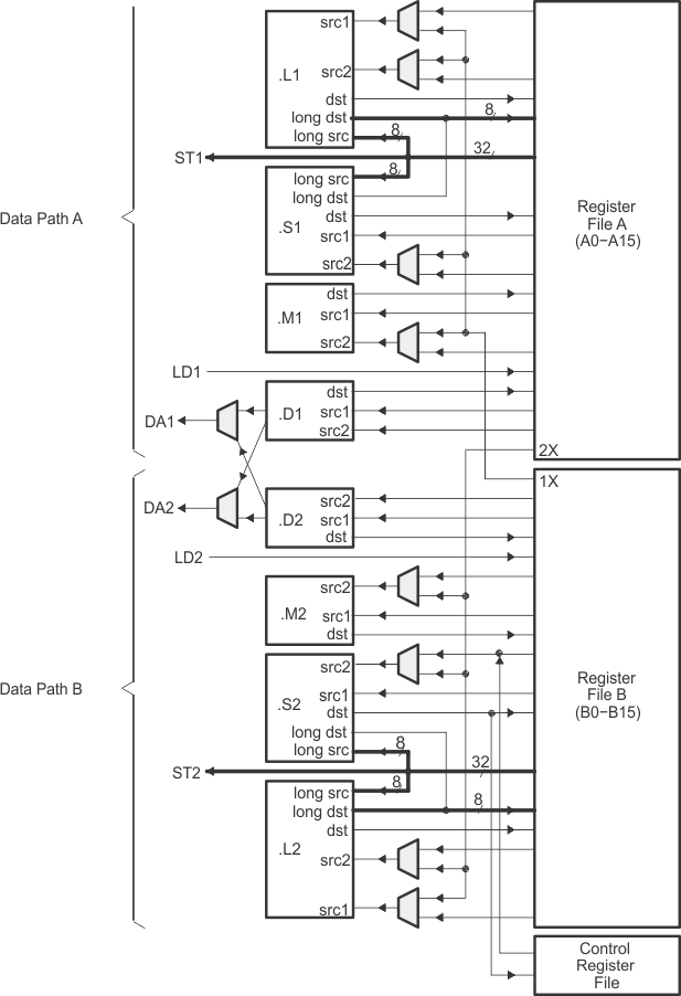 Figure 53. SMJ320C62x CPU (DSP Core) Data Paths
9.2.3 Clock PLL
Most of the internal C6203 clocks are generated from a single source through the CLKIN pin. This source clock either drives the PLL, which multiplies the source clock in frequency to generate the internal CPU clock, or bypasses the PLL to become the internal CPU clock.
To use the PLL to generate the CPU clock, the external PLL filter circuit must be properly designed. Figure 54, and Table 3 through Table 17 show the external PLL circuitry for either x1 (PLL bypass) or x4 PLL multiply modes. Figure 55 shows the external PLL circuitry for a system with only x1 (PLL bypass) mode.
To minimize the clock jitter, a single clean power supply should power both the C6203 device and the external clock oscillator circuit. Noise coupling into PLLF directly impacts PLL clock jitter. Observe the minimum CLKIN rise and fall times. For the input clock timing requirements, see the input and output clocks in Specifications. Table 2 lists some examples of compatible CLKIN external clock sources:
Table 2. Compatible CLKIN External Clock Sources
| COMPATIBLE PARTS FOR EXTERNAL CLOCK SOURCES (CLKIN) | PART NUMBER | MANUFACTURER |
|---|---|---|
| Oscillators | JITO-2 | Fox Electronix |
| STA series, ST4100 series | SaRonix Corporation | |
| SG-636 | Epson America | |
| 342 | Corning Frequency Control | |
| PLL | MK1711-S, ICS525-02 | Integrated Circuit Systems |
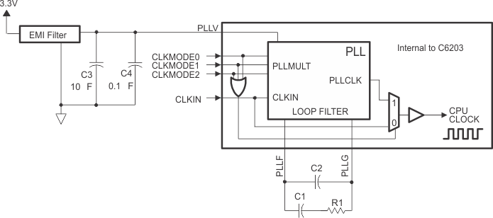
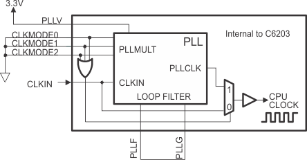
Table 3. PLL Multiply and Bypass (x1) Options(1)
| BIT (PIN NO.) | CLKMODE2 (G12) | CLKMODE1 (G10) | CLKMODE0 (C12) | DEVICES AND PLL CLOCK OPTIONS |
|---|---|---|---|---|
| C6203 (GLP) | ||||
| Value | 0 | 0 | 0 | Bypass (x1) |
| 0 | 0 | 1 | x4 | |
| 0 | 1 | 0 | x8 | |
| 0 | 1 | 1 | x10 | |
| 1 | 0 | 0 | x6 | |
| 1 | 0 | 1 | x9 | |
| 1 | 1 | 0 | x7 | |
| 1 | 1 | 1 | x11 |
9.3 Register Maps
9.3.1 Memory Map Summary
Table 4 shows the memory map address ranges of the C6203 device. The C6203 device has the capability of a MAP 0 or MAP 1 memory block configuration. These memory block configurations are set up at reset by the boot configuration pins (generically called BOOTMODE[4:0]). For the C6203 device, the BOOTMODE configuration is handled, at reset, by the expansion bus module (specifically XD[4:0] pins). For more detailed information on the C6203 device settings, which include the device boot mode configuration at reset and other device-specific configurations, see the TMS320C6000 Peripherals Reference Guide (SPRU190) for information regarding boot configuration.
Table 4. 320C6203 Memory Map Summary
| MEMORY BLOCK DESCRIPTION | BLOCK SIZE (BYTES) | HEX ADDRESS RANGE | |
|---|---|---|---|
| MAP 0 | MAP 1 | ||
| External Memory Interface (EMIF) CE0 | Internal Program RAM | 384K | 0000_0000 – 0005_FFFF |
| EMIF CE0 | Reserved | 4M – 384K | 0006_0000 – 003F_FFFF |
| EMIF CE0 | EMIF CE0 | 12M | 0040_0000 – 00FF_FFFF |
| EMIF CE1 | EMIF CE0 | 4M | 0100_0000 – 013F_FFFF |
| Internal Program RAM | EMIF CE1 | 384K | 0140_0000 – 0145_FFFF |
| Reserved | EMIF CE1 | 4M – 384K | 0146_0000 – 017F_FFFF |
| EMIF Registers | 256K | 0180_0000 – 0183_FFFF | |
| DMA Controller Registers | 256K | 0184_0000 – 0187_FFFF | |
| Expansion Bus Registers | 256K | 0188_0000 – 018B_FFFF | |
| McBSP 0 Registers | 256K | 018C_0000 – 018F_FFFF | |
| McBSP 1 Registers | 256K | 0190_0000 – 0193_FFFF | |
| Timer 0 Registers | 256K | 0194_0000 – 0197_FFFF | |
| Timer 1 Registers | 256K | 0198_0000 – 019B_FFFF | |
| Interrupt Selector Registers | 512 | 019C_0000 – 019C_01FF | |
| Power-Down Registers | 256K – 512 | 019C_0200 – 019F_FFFF | |
| Reserved | 256K | 01A0_0000 – 01A3_FFFF | |
| McBSP 2 Registers | 256K | 01A4_0000 – 01A7_FFFF | |
| Reserved | 5.5M | 01A8_0000 – 01FF_FFFF | |
| EMIF CE2 | 16M | 0200_0000 – 02FF_FFFF | |
| EMIF CE3 | 16M | 0300_0000 – 03FF_FFFF | |
| Reserved | 1G – 64M | 0400_0000 – 3FFF_FFFF | |
| Expansion bus XCE0 | 256M | 4000_0000 – 4FFF_FFFF | |
| Expansion bus XCE1 | 256M | 5000_0000 – 5FFF_FFFF | |
| Expansion bus XCE2 | 256M | 6000_0000 – 6FFF_FFFF | |
| Expansion bus XCE3 | 256M | 7000_0000 – 7FFF_FFFF | |
| Internal Data RAM | 512K | 8000_0000 – 8007_FFFF | |
| Reserved | 2G – 512K | 8008_0000 – FFFF_FFFF | |
9.3.2 Peripheral Register Descriptions
Table 5 through Table 14 identify the peripheral registers for the C6203 device by their register names, acronyms, and hex address or hex address range. For more detailed information on the register contents, bit names, and their descriptions, see the TMS320C6000 Peripherals Reference Guide (SPRU190).
Table 5. EMIF Registers
| HEX ADDRESS RANGE | ACRONYM | REGISTER NAME | COMMENTS |
|---|---|---|---|
| 0180 0000 | GBLCTL | EMIF global control | |
| 0180 0004 | CECTL1 | EMIF CE1 space control | External or internal; dependent on MAP0 or MAP1 configuration (selected by the MAP bit in the EMIF GBLCTL register |
| 0180 0008 | CECTL0 | EMIF CE0 space control | External or internal; dependent on MAP0 or MAP1 configuration (selected by the MAP bit in the EMIF GBLCTL register |
| 0180 000C | − | Reserved | |
| 0180 0010 | CECTL2 | EMIF CE2 space control | Corresponds to EMIF CE2 memory space: [0200 0000 − 02FF FFFF] |
| 0180 0014 | CECTL3 | EMIF CE3 space control | Corresponds to EMIF CE3 memory space: [0300 0000 − 03FF FFFF] |
| 0180 0018 | SDCTL | EMIF SDRAM control | |
| 0180 001C | SDTIM | EMIF SDRAM refresh control | |
| 0180 0020 − 0180 0054 | − | Reserved | |
| 0180 0058 − 0183 FFFF | – | Reserved |
Table 6. DMA Registers
| HEX ADDRESS RANGE | ACRONYM | REGISTER NAME |
|---|---|---|
| 0184 0000 | PRICTL0 | DMA channel 0 primary control |
| 0184 0004 | PRICTL2 | DMA channel 2 primary control |
| 0184 0008 | SECCTL0 | DMA channel 0 secondary control |
| 0184 000C | SECCTL2 | DMA channel 2 secondary control |
| 0184 0010 | SRC0 | DMA channel 0 source address |
| 0184 0014 | SRC2 | DMA channel 2 source address |
| 0184 0018 | DST0 | DMA channel 0 destination address |
| 0184 001C | DST2 | DMA channel 2 destination address |
| 0184 0020 | XFRCNT0 | DMA channel 0 transfer counter |
| 0184 0024 | XFRCNT2 | DMA channel 2 transfer counter |
| 0184 0028 | GBLCNTA | DMA global count reload register A |
| 0184 002C | GBLCNTB | DMA global count reload register B |
| 0184 0030 | GBLIDXA | DMA global index register A |
| 0184 0034 | GBLIDXB | DMA global index register B |
| 0184 0038 | GBLADDRA | DMA global address register A |
| 0184 003C | GBLADDRB | DMA global address register B |
| 0184 0040 | PRICTL1 | DMA channel 1 primary control |
| 0184 0044 | PRICTL3 | DMA channel 3 primary control |
| 0184 0048 | SECCTL1 | DMA channel 1 secondary control |
| 0184 004C | SECCTL3 | DMA channel 3 secondary control |
| 0184 0050 | SRC1 | DMA channel 1 source address |
| 0184 0054 | SRC3 | DMA channel 3 source address |
| 0184 0058 | DST1 | DMA channel 1 destination address |
| 0184 005C | DST3 | DMA channel 3 destination address |
| 0184 0060 | XFRCNT1 | DMA channel 1 transfer counter |
| 0184 0064 | XFRCNT3 | DMA channel 3 transfer counter |
| 0184 0068 | GBLADDRC | DMA global address register C |
| 0184 006C | GBLADDRD | DMA global address register D |
| 0184 0070 | AUXCTL | DMA auxiliary control register |
| 0184 0074 − 0187 FFFF | – | Reserved |
Table 7. Expansion Bus Registers
| HEX ADDRESS RANGE | ACRONYM | REGISTER NAME | COMMENTS |
|---|---|---|---|
| 0188 0000 | XBGC | Expansion bus global control register | |
| 0188 0004 | XCECTL1 | XCE1 space control register | Corresponds to expansion bus XCE0 memory space: [4000 0000 − 4FFF FFFF] |
| 0188 0008 | XCECTL0 | XCE0 space control register | Corresponds to expansion bus XCE1 memory space: [5000 0000 − 5FFF FFFF] |
| 0188 000C | XBHC | Expansion bus host port interface control register | DSP read/write access only |
| 0188 0010 | XCECTL2 | XCE2 space control register | Corresponds to expansion bus XCE2 memory space: [6000 0000 − 6FFF FFFF] |
| 0188 0014 | XCECTL3 | XCE3 space control register | Corresponds to expansion bus XCE3 memory space: [7000 0000 − 7FFF FFFF] |
| 0188 0018 | − | Reserved | |
| 0188 001C | − | Reserved | |
| 0188 0020 | XBIMA | Expansion bus internal master address register | DSP read/write access only |
| 0188 0024 | XBEA | Expansion bus external address register | DSP read/write access only |
| 0188 0028 − 018B FFFF | − | Reserved | |
| − | XBISA | Expansion bus internal slave address | |
| − | XBD | Expansion bus data |
Table 8. Interrupt Selector Registers
| HEX ADDRESS RANGE | ACRONYM | REGISTER NAME | COMMENTS |
|---|---|---|---|
| 019C 0000 | MUXH | Interrupt multiplexer high | Selects which interrupts drive CPU interrupts 10 to 15 (INT10 to INT15) |
| 019C 0004 | MUXL | Interrupt multiplexer low | Selects which interrupts drive CPU interrupts 4 to 9 (INT04 to INT09) |
| 019C 0008 | EXTPOL | External interrupt polarity | Sets the polarity of the external interrupts (EXT_INT4−EXT_INT7) |
| 019C 000C − 019C 01FF | − | Reserved | |
| 019C 0200 | PDCTL | Peripheral power-down control register | |
| 019C 0204 − 019F FFFF | − | Reserved |
Table 9. Peripheral Power-Down Control Register
| HEX ADDRESS RANGE | ACRONYM | REGISTER NAME |
|---|---|---|
| 019C 0200 | PDCTL | Peripheral power-down control register |
Table 10. McBSP 0 Registers
| HEX ADDRESS RANGE | ACRONYM | REGISTER NAME | COMMENTS |
|---|---|---|---|
| 018C 0000 | DRR0 | McBSP0 data receive register | The CPU and DMA/EDMA controller can only read this register; they cannot write to it. |
| 018C 0004 | DXR0 | McBSP0 data transmit register | |
| 018C 0008 | SPCR0 | McBSP0 serial port control register | |
| 018C 000C | RCR0 | McBSP0 receive control register | |
| 018C 0010 | XCR0 | McBSP0 transmit control register | |
| 018C 0014 | SRGR0 | McBSP0 sample rate generator register | |
| 018C 0018 | MCR0 | McBSP0 multichannel control register | |
| 018C 001C | RCER0 | McBSP0 receive channel enable register | |
| 018C 0020 | XCER0 | McBSP0 transmit channel enable register | |
| 018C 0024 | PCR0 | McBSP0 pin control register | |
| 018C 0028 − 018F FFFF | – | Reserved |
Table 11. McBSP 1 Registers
| HEX ADDRESS RANGE | ACRONYM | REGISTER NAME | COMMENTS |
|---|---|---|---|
| 0190 0000 | DRR1 | Data receive register | The CPU and DMA/EDMA controller can only read this register; they cannot write to it. |
| 0190 0004 | DXR1 | McBSP1 data transmit register | |
| 0190 0008 | SPCR1 | McBSP1 serial port control register | |
| 0190 000C | RCR1 | McBSP1 receive control register | |
| 0190 0010 | XCR1 | McBSP1 transmit control register | |
| 0190 0014 | SRGR1 | McBSP1 sample rate generator register | |
| 0190 0018 | MCR1 | McBSP1 multichannel control register | |
| 0190 001C | RCER1 | McBSP1 receive channel enable register | |
| 0190 0020 | XCER1 | McBSP1 transmit channel enable register | |
| 0190 0024 | PCR1 | McBSP1 pin control register | |
| 0190 0028 − 0193 FFFF | – | Reserved |
Table 12. McBSP 2 Registers
| HEX ADDRESS RANGE | ACRONYM | REGISTER NAME | COMMENTS |
|---|---|---|---|
| 01A4 0000 | DRR2 | McBSP2 data receive register | The CPU and DMA/EDMA controller can only read this register; they cannot write to it. |
| 01A4 0004 | DXR2 | McBSP2 data transmit register | |
| 01A4 0008 | SPCR2 | McBSP2 serial port control register | |
| 01A4 000C | RCR2 | McBSP2 receive control register | |
| 01A4 0010 | XCR2 | McBSP2 transmit control register | |
| 01A4 0014 | SRGR2 | McBSP2 sample rate generator register | |
| 01A4 0018 | MCR2 | McBSP2 multichannel control register | |
| 01A4 001C | RCER2 | McBSP2 receive channel enable register | |
| 01A4 0020 | XCER2 | McBSP2 transmit channel enable register | |
| 01A4 0024 | PCR2 | McBSP2 pin control register | |
| 01A4 0028 − 01A7 FFFF | – | Reserved |
Table 13. Timer 0 Registers
| HEX ADDRESS RANGE | ACRONYM | REGISTER NAME | COMMENTS |
|---|---|---|---|
| 0194 0000 | CTL0 | Timer 0 control register | Determines the operating mode of the timer, monitors the timer status, and controls the function of the TOUT pin. |
| 0194 0004 | PRD0 | Timer 0 period register | Contains the number of timer input clock cycles to count. This number controls the TSTAT signal frequency. |
| 0194 0008 | CNT0 | Timer 0 counter register | Contains the current value of the incrementing counter. |
| 0194 000C − 0197 FFFF | − | Reserved |
Table 14. Timer 1 Registers
| HEX ADDRESS RANGE | ACRONYM | REGISTER NAME | COMMENTS |
|---|---|---|---|
| 0198 0000 | CTL1 | Timer 1 control register | Determines the operating mode of the timer, monitors the timer status, and controls the function of the TOUT pin. |
| 0198 0004 | PRD1 | Timer 1 period register | Contains the number of timer input clock cycles to count. This number controls the TSTAT signal frequency. |
| 0198 0008 | CNT1 | Timer 1 counter register | Contains the current value of the incrementing counter. |
| 0198 000C − 019B FFFF | − | Reserved |
The C6203 DMA supports up to four independent programmable DMA channels, plus an auxiliary channel used for servicing the HPI module. The four main DMA channels can be read/write synchronized based on the events shown in Table 15. Selection of these events is done by the RSYNC and WSYNC fields in the Primary Control registers of the specific DMA channel. For more detailed information on the DMA module, associated channels, and event-synchronization, see the TMS320C6000 Peripherals Reference Guide (SPRU190).
Table 15. 320C6203 DMA Synchronization Events
| DMA EVENT NUMBER (BINARY) | EVENT NAME | EVENT DESCRIPTION |
|---|---|---|
| 00000 | Reserved | Reserved |
| 00001 | TINT0 | Timer 0 interrupt |
| 00010 | TINT1 | Timer 1 interrupt |
| 00011 | SD_INT | EMIF SDRAM timer interrupt |
| 00100 | EXT_INT4 | External interrupt pin 4 |
| 00101 | EXT_INT5 | External interrupt pin 5 |
| 00110 | EXT_INT6 | External interrupt pin 6 |
| 00111 | EXT_INT7 | External interrupt pin 7 |
| 01000 | DMA_INT0 | DMA channel 0 interrupt |
| 01001 | DMA_INT1 | DMA channel 1 interrupt |
| 01010 | DMA_INT2 | DMA channel 2 interrupt |
| 01011 | DMA_INT3 | DMA channel 3 interrupt |
| 01100 | XEVT0 | McBSP0 transmit event |
| 01101 | REVT0 | McBSP0 receive event |
| 01110 | XEVT1 | McBSP1 transmit event |
| 01111 | REVT1 | McBSP1 receive event |
| 10000 | DSP_INT | Host processor-to-DSP interrupt |
| 10001 | XEVT2 | McBSP2 transmit event |
| 10010 | REVT2 | McBSP2 receive event |
| 10011 − 11111 | Reserved | Reserved. Not used. |
9.3.3 Interrupt Sources and Interrupt Selector
The C62x DSP core supports 16 prioritized interrupts, which are listed in Table 16. The highest-priority interrupt is INT_00 (dedicated to RESET) while the lowest-priority interrupt is INT_15. The first four interrupts (INT_00 to INT_03) are non-maskable and fixed. The remaining interrupts (INT_04 to INT_15) are maskable and default to the interrupt source specified in Table 16. The interrupt source for interrupts 4 to 15 can be programmed by modifying the selector value (binary value) in the corresponding fields of the Interrupt Selector Control registers: MUXH (address 0x019C0000) and MUXL (address 0x019C0004).
Table 16. C6203 DSP Interrupts
| CPU INTERRUPT NUMBER | INTERRUPT SELECTOR CONTROL REGISTER | SELECTOR VALUE (BINARY) | INTERRUPT EVENT | INTERRUPT SOURCE |
|---|---|---|---|---|
| INT_00(1) | − | − | RESET | |
| INT_01(1) | − | − | NMI | |
| INT_02(1) | − | − | Reserved | Reserved. Do not use. |
| INT_03(1) | − | − | Reserved | Reserved. Do not use. |
| INT_04(2) | MUXL[4:0] | 00100 | EXT_INT4 | External interrupt pin 4 |
| INT_05(2) | MUXL[9:5] | 00101 | EXT_INT5 | External interrupt pin 5 |
| INT_06(2) | MUXL[14:10] | 00110 | EXT_INT6 | External interrupt pin 6 |
| INT_07(2) | MUXL[20:16] | 00111 | EXT_INT7 | External interrupt pin 7 |
| INT_08(2) | MUXL[25:21] | 01000 | DMA_INT0 | DMA channel 0 interrupt |
| INT_09(2) | MUXL[30:26] | 01001 | DMA_INT1 | DMA channel 1 interrupt |
| INT_10(2) | MUXH[4:0] | 00011 | SD_INT | EMIF SDRAM timer interrupt |
| INT_11(2) | MUXH[9:5] | 01010 | DMA_INT2 | DMA channel 2 interrupt |
| INT_12(2) | MUXH[14:10] | 01011 | DMA_INT3 | DMA channel 3 interrupt |
| INT_13(2) | MUXH[20:16] | 00000 | DSP_INT | Host-processor-to-DSP interrupt |
| INT_14(2) | MUXH[25:21] | 00001 | TINT0 | Timer 0 interrupt |
| INT_15(2) | MUXH[30:26] | 00010 | TINT1 | Timer 1 interrupt |
| − | − | 01100 | XINT0 | McBSP0 transmit interrupt |
| − | − | 01101 | RINT0 | McBSP0 receive interrupt |
| − | − | 01110 | XINT1 | McBSP1 transmit interrupt |
| − | − | 01111 | RINT1 | McBSP1 receive interrupt |
| − | − | 10000 | Reserved | Reserved. Not used. |
| − | − | 10001 | XINT2 | McBSP2 transmit interrupt |
| − | − | 10010 | RINT2 | McBSP2 receive interrupt |
| − | − | 10011 − 11111 | Reserved | Reserved. Do not use. |