SLLSF98 December 2018 SN55HVD233-SEP
PRODUCTION DATA.
- 1 Features
- 2 Applications
- 3 Description
- 4 Revision History
- 5 Description (continued)
- 6 Pin Configuration and Functions
-
7 Specifications
- 7.1 Absolute Maximum Ratings
- 7.2 ESD Ratings
- 7.3 Recommended Operating Conditions
- 7.4 Thermal Information
- 7.5 Driver Electrical Characteristics
- 7.6 Receiver Electrical Characteristics
- 7.7 Driver Switching Characteristics
- 7.8 Receiver Switching Characteristics
- 7.9 Device Switching Characteristics
- 7.10 Typical Characteristics
- 8 Parameter Measurement Information
- 9 Detailed Description
- 10Application and Implementation
- 11Power Supply Recommendations
- 12Layout
- 13Device and Documentation Support
- 14Mechanical, Packaging, and Orderable Information
Package Options
Mechanical Data (Package|Pins)
- D|8
Thermal pad, mechanical data (Package|Pins)
Orderable Information
9.3.3 CAN Bus States
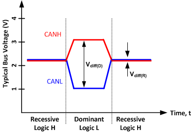
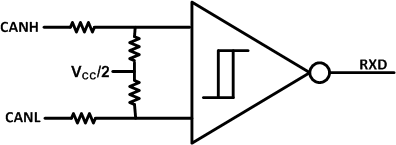
The CAN bus has two states during powered operation of the device: dominant and recessive. A dominant bus state is when the bus is driven differentially, corresponding to a logic low on the D and R pin. A recessive bus state is when the bus is biased to VCC / 2 through the high-resistance internal input resistors RIN of the receiver, corresponding to a logic high on the D and R pins (see Figure 25 and Figure 26).
 Figure 25. Bus States (Physical Bit Representation)
  Figure 26. Simplified Recessive Common Mode Bias and Receiver