SLLS261N July 1997 – April 2021 SN55LVDS31 , SN65LVDS31 , SN65LVDS3487 , SN65LVDS9638
PRODUCTION DATA
- 1 Features
- 2 Applications
- 3 Description
- 4 Revision History
- 5 Description (Continued)
- 6 Pin Configuration and Functions
-
7 Specifications
- 7.1 Absolute Maximum Ratings (1)
- 7.2 ESD Ratings
- 7.3 Recommended Operating Conditions
- 7.4 Thermal Information
- 7.5 Electrical Characteristics: SN55LVDS31
- 7.6 Electrical Characteristics: SN65LVDSxxxx
- 7.7 Switching Characteristics: SN55LVDS31
- 7.8 Switching Characteristics: SN65LVDSxxxx
- 7.9 Typical Characteristics
- 8 Parameter Measurement Information
- 9 Detailed Description
- 10Application and Implementation
- 11Power Supply Recommendations
- 12Layout
- 13Device and Documentation Support
- 14Mechanical, Packaging, and Orderable Information
Package Options
Refer to the PDF data sheet for device specific package drawings
Mechanical Data (Package|Pins)
- W|16
- J|16
- FK|20
Thermal pad, mechanical data (Package|Pins)
Orderable Information
9.3.4 Driver Equivalent Schematics
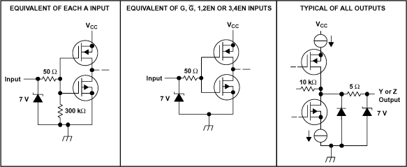
The driver input is represented by a CMOS inverter stage with a 7-V Zener diode. The input stage is high-impedance, and includes an internal pulldown to ground. If the driver input is left open, the driver input provides a low-level signal to the rest of the driver circuitry, resulting in a low-level signal at the driver output pins. The Zener diode provides ESD protection. The driver output stage is a differential pair, one half of which is shown in Figure 9-1. Like the input stage, the driver output includes Zener diodes for ESD protection. The schematic shows an output stage that includes a set of current sources (nominally 3.5 mA) that are connected to the output load circuit based upon the input stage signal. To the first order, the SNx5LVDSxx output stage acts a constant-current source.
 Figure 9-1 Equivalent Input and Output Schematic Diagrams