SLLSEP9I september 2015 – august 2023 SN6505A , SN6505B
PRODUCTION DATA
- 1
- 1 Features
- 2 Applications
- 3 Description
- 4 Revision History
- 5 Pin Configuration and Functions
- 6 Specifications
- 7 Parameter Measurement Information
- 8 Detailed Description
- 9 Application and Implementation
- 10Power Supply Recommendations
- 11Layout
- 12Device and Documentation Support
- 13Mechanical, Packaging, and Orderable Information
Package Options
Mechanical Data (Package|Pins)
- DBV|6
Thermal pad, mechanical data (Package|Pins)
Orderable Information
3 Description
The SN6505x is a low-noise,
low-EMI push-pull transformer driver, specifically designed for small form factor,
isolated power supplies. It drives low-profile, center-tapped transformers from a
2.25 V to
5 V DC power supply. Ultra-low noise and EMI are achieved by slew rate control of the output
switch voltage and through Spread Spectrum Clocking (SSC). The SN6505x consists of an oscillator followed by a gate drive circuit that
provides the complementary output signals to drive ground-referenced N-channel power
switches. The device includes two 1-A Power-MOSFET switches to ensure start-up under
heavy loads. The switching clock can also be provided externally for accurate
placement of switcher harmonics, or when operating with multiple transformer
drivers. The internal protection features include a 1.7 A current limiting,
under-voltage lockout, thermal shutdown, and break-before-make circuitry. SN6505x includes
a soft-start feature that prevents high inrush current during power up with large
load capacitors.
SN6505A has a 160 kHz internal oscillator for applications that need to
minimize emissions whereas SN6505Bhas
a 420 kHz internal oscillators for applications that require higher
efficiency and smaller transformer size. The SN6505x is available in a
small 6-pin SOT23/DBV package. The device operation is characterized for a
temperature range from –55°C to 125°C.
| PART NUMBER | PACKAGE | BODY SIZE (NOM) |
|---|---|---|
| SN6505A | SOT23 (6 Pin) | 2.90 mm × 1.60 mm |
| SN6505B |
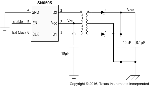
 Simplified Schematic