SLLSEW7A December   2016  – June 2018 SN65DSI83-Q1

PRODUCTION DATA.  

  1. Features
  2. Applications
  3. Description
    1.     SN65DSI83-Q1 Schematic
  4. Revision History
  5. Pin Configuration and Functions
    1.     Pin Functions
  6. Specifications
    1. 6.1 Absolute Maximum Ratings
    2. 6.2 ESD Ratings
    3. 6.3 Recommended Operating Conditions
    4. 6.4 Thermal Information
    5. 6.5 Electrical Characteristics
    6. 6.6 Switching Characteristics
  7. Parameter Measurement Information
  8. Detailed Description
    1. 8.1 Overview
    2. 8.2 Functional Block Diagram
    3. 8.3 Feature Description
      1. 8.3.1 Clock Configurations and Multipliers
      2. 8.3.2 ULPS
      3. 8.3.3 LVDS Pattern Generation
      4. 8.3.4 Reset Implementation
      5. 8.3.5 Initialization Sequence
      6. 8.3.6 LVDS Output Formats
      7. 8.3.7 DSI Lane Merging
      8. 8.3.8 DSI Pixel Stream Packets
      9. 8.3.9 DSI Video Transmission Specifications
    4. 8.4 Programming
      1. 8.4.1 Local I2C Interface Overview
    5. 8.5 Register Maps
      1. 8.5.1 Control and Status Registers Overview
        1. 8.5.1.1 CSR Bit Field Definitions – ID Registers
          1. 8.5.1.1.1 Registers 0x00 – 0x08
            1. Table 4. Registers 0x00 – 0x08 Field Descriptions
        2. 8.5.1.2 CSR Bit Field Definitions – Reset and Clock Registers
          1. 8.5.1.2.1 Register 0x09
            1. Table 5. Register 0x09 Field Descriptions
          2. 8.5.1.2.2 Register 0x0A
            1. Table 6. Register 0x0A Field Descriptions
          3. 8.5.1.2.3 Register 0x0B
            1. Table 7. Register 0x0B Field Descriptions
          4. 8.5.1.2.4 Register 0x0D
            1. Table 8. Register 0x0D Field Descriptions
        3. 8.5.1.3 CSR Bit Field Definitions – DSI Registers
          1. 8.5.1.3.1 Register 0x10
            1. Table 9. Register 0x10 Field Descriptions
          2. 8.5.1.3.2 Register 0x11
            1. Table 10. Register 0x11 Field Descriptions
          3. 8.5.1.3.3 Register 0x12
            1. Table 11. Register 0x12 Field Descriptions
        4. 8.5.1.4 CSR Bit Field Definitions – LVDS Registers
          1. 8.5.1.4.1 Register 0x18
            1. Table 12. Register 0x18 Field Descriptions
          2. 8.5.1.4.2 Register 0x19
            1. Table 13. Register 0x19 Field Descriptions
          3. 8.5.1.4.3 Register 0x1A
            1. Table 14. Register 0x1A Field Descriptions
          4. 8.5.1.4.4 Register 0x1B
            1. Table 15. Register 0x1B Field Descriptions
        5. 8.5.1.5 CSR Bit Field Definitions – Video Registers
          1. 8.5.1.5.1  Register 0x20
            1. Table 16. Register 0x20 Field Descriptions
          2. 8.5.1.5.2  Register 0x21
            1. Table 17. Register 0x21 Field Descriptions
          3. 8.5.1.5.3  Register 0x24
            1. Table 18. Register 0x24 Field Descriptions
          4. 8.5.1.5.4  Register 0x25
            1. Table 19. Register 0x25 Field Descriptions
          5. 8.5.1.5.5  Register 0x28
            1. Table 20. Register 0x28 Field Descriptions
          6. 8.5.1.5.6  Register 0x29
            1. Table 21. Register 0x29 Field Descriptions
          7. 8.5.1.5.7  Register 0x2C
            1. Table 22. Register 0x2C Field Descriptions
          8. 8.5.1.5.8  Register 0x2D
            1. Table 23. Register 0x2D Field Descriptions
          9. 8.5.1.5.9  Register 0x30
            1. Table 24. Register 0x30 Field Descriptions
          10. 8.5.1.5.10 Register 0x31
            1. Table 25. Register 0x31 Field Descriptions
          11. 8.5.1.5.11 Register 0x34
            1. Table 26. Register 0x34 Field Descriptions
          12. 8.5.1.5.12 Register 0x36
            1. Table 27. Register 0x36 Field Descriptions
          13. 8.5.1.5.13 Register 0x38
            1. Table 28. Register 0x38 Field Descriptions
          14. 8.5.1.5.14 Register 0x3A
            1. Table 29. Register 0x3A Field Descriptions
          15. 8.5.1.5.15 Register 0x3C
            1. Table 30. Register 0x3C Field Descriptions
        6. 8.5.1.6 CSR Bit Field Definitions – IRQ Registers
          1. 8.5.1.6.1 Register 0xE0
            1. Table 31. Register 0xE0 Field Descriptions
          2. 8.5.1.6.2 Register 0xE1
            1. Table 32. Register 0xE1 Field Descriptions
          3. 8.5.1.6.3 Register 0xE5
            1. Table 33. Register 0xE5 Field Descriptions
  9. Application and Implementation
    1. 9.1 Application Information
      1. 9.1.1 Video STOP and Restart Sequence
      2. 9.1.2 Reverse LVDS Pin Order Option
      3. 9.1.3 IRQ Usage
    2. 9.2 Typical Application
      1. 9.2.1 Design Requirements
      2. 9.2.2 Detailed Design Procedure
        1. 9.2.2.1 Example Script
      3. 9.2.3 Application Curve
  10. 10Power Supply Recommendations
    1. 10.1 VCC Power Supply
    2. 10.2 VCORE Power Supply
  11. 11Layout
    1. 11.1 Layout Guidelines
      1. 11.1.1 Package Specific
      2. 11.1.2 Differential Pairs
      3. 11.1.3 Ground
    2. 11.2 Layout Example
  12. 12Device and Documentation Support
    1. 12.1 Documentation Support
      1. 12.1.1 Related Documentation
    2. 12.2 Receiving Notification of Documentation Updates
    3. 12.3 Community Resource
    4. 12.4 Trademarks
    5. 12.5 Electrostatic Discharge Caution
    6. 12.6 Glossary
  13. 13Mechanical, Packaging, and Orderable Information

Package Options

Mechanical Data (Package|Pins)
Thermal pad, mechanical data (Package|Pins)
Orderable Information

DSI Video Transmission Specifications

The SN65DSI83-Q1 supports burst video mode and non-burst video mode with sync events or with sync pulses packet transmission as described in the DSI specification. The burst mode supports time-compressed pixel stream packets that leave added time per scan line for power savings LP mode. The SN65DSI83-Q1 requires a transition to LP mode once per frame to enable PHY synchronization with the DSI host processor; however, for a robust and low-power implementation, the transition to LP mode is recommended on every video line.

Figure 17 shows the DSI video transmission applied to SN65DSI83-Q1 applications. In all applications, the LVDS output rate must be less than or equal to the DSI input rate. The first line of a video frame shall start with a VSS packet, and all other lines start with VSE or HSS. The position of the synchronization packets in time is of utmost importance since this has a direct impact on the visual performance of the display panel; that is, these packets generate the HS and VS (horizontal and vertical sync) signals on the LVDS interface after the delay programmed into CHA_SYNC_DELAY_LOW/HIGH (CSR 0×28.7:0 and 0×29.3:0).

As required in the DSI specification, the SN65DSI83-Q1 requires that pixel stream packets contain an integer number of pixels (i.e. end on a pixel boundary); it is recommended to transmit an entire scan line on one pixel stream packet. When a scan line is broken in to multiple packets, inter-packet latency shall be considered such that the video pipeline (ie. pixel queue or partial line buffer) does not run empty (i.e. under-run); during scan line processing, if the pixel queue runs empty, the SNDSI83-Q1 transmits zero data (18’b0 or 24’b0) on the LVDS interface.

NOTE

When the HS clock is used as a source for the LVDS pixel clock, the LP mode transitions apply only to the data lanes, and the DSI clock lane remains in the HS mode during the entire video transmission.

The SN65DSI83-Q1 does not support the DSI Virtual Channel capability or reverse direction (peripheral to processor) transmissions.
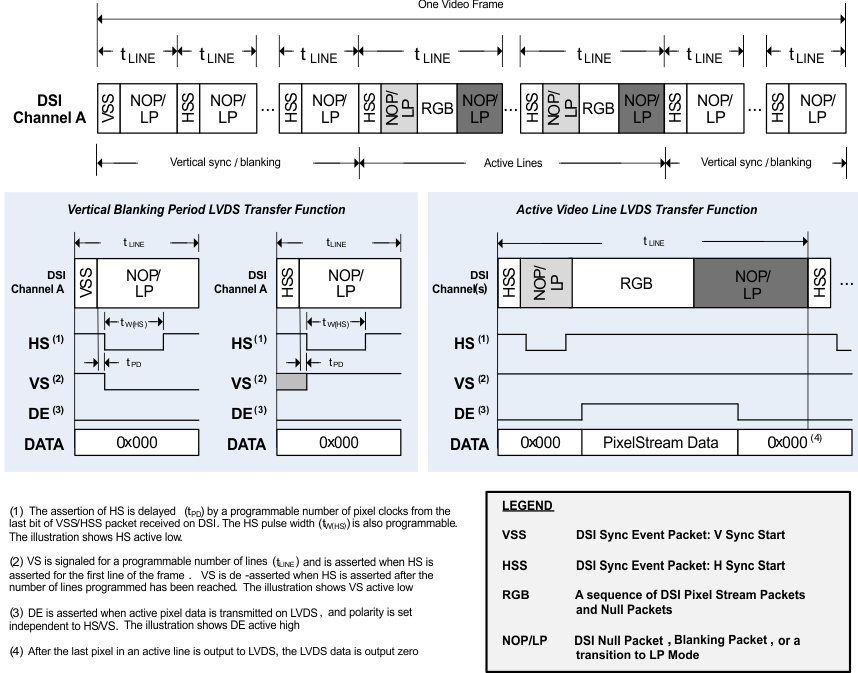
SN65DSI83-Q1 DSI_channel_tranmission_sllsej4.gifFigure 17. DSI Channel Transmission and Transfer Function