SLLS934F November 2008 – November 2015 SN65HVD11-HT
PRODUCTION DATA.
- 1 Features
- 2 Applications
- 3 Description
- 4 Revision History
- 5 Pin Configuration and Functions
- 6 Specifications
- 7 Parameter Measurement Information
- 8 Detailed Description
- 9 Application and Implementation
- 10Power Supply Recommendations
- 11Layout
- 12Device and Documentation Support
- 13Mechanical, Packaging, and Orderable Information
Package Options
Mechanical Data (Package|Pins)
Thermal pad, mechanical data (Package|Pins)
Orderable Information
9 Application and Implementation
NOTE
Information in the following applications sections is not part of the TI component specification, and TI does not warrant its accuracy or completeness. TI’s customers are responsible for determining suitability of components for their purposes. Customers should validate and test their design implementation to confirm system functionality.
9.1 Application Information
The SN65HVD11-HT is a half-duplex RS-485 transceiver commonly used for asynchronous data transmissions. The driver and receiver enable pins allow for the configuration of different operating modes.
 Figure 22. Half-Duplex Transceiver Configurations
- Using independent enable lines provides the most flexible control as it allows for the driver and the receiver to be turned on and off individually. While this configuration requires two control lines, it allows for selective listening into the bus traffic, whether the driver is transmitting data or not.
- Combining the enable signals simplifies the interface to the controller by forming a single direction-control signal. In this configuration, the transceiver operates as a driver when the direction-control line is high, and as a receiver when the direction-control line is low.
- Only one line is required when connecting the receiver-enable input to ground and controlling only the driver-enable input. In this configuration, a node not only receives the data from the bus, but also the data it sends and can verify that the correct data have been transmitted.
9.2 Typical Application
An RS-485 bus consists of multiple transceivers connected in parallel to a bus cable. To eliminate line reflections, each cable end is terminated with a termination resistor, RT, whose value matches the characteristic impedance, Z0, of the cable. This method, known as parallel termination, allows for higher data rates over a longer cable length.
 Figure 23. Typical RS-485 Network With Half-Duplex Transceivers
9.2.1 Design Requirements
RS-485 is a robust electrical standard suitable for long-distance networking that may be used in a wide range of applications with varying requirements, such as distance, data rate, and number of nodes.
9.2.1.1 Data Rate and Bus Length
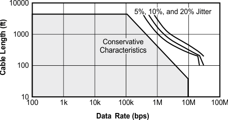
There is an inverse relationship between data rate and bus length, meaning the higher the data rate, the shorter the cable length; and conversely, the lower the data rate, the longer the cable may be without introducing data errors. While most RS-485 systems use data rates between 10 kbps and 100 kbps, some applications require data rates up to 250 kbps at distances of 4000 feet and longer. Longer distances are possible by allowing for small signal jitter of up to 5 or 10%.
 Figure 24. Cable Length vs Data Rate Characteristic
9.2.1.2 Stub Length
When connecting a node to the bus, the distance between the transceiver inputs and the cable trunk, known as the stub, should be as short as possible. Stubs present a nonterminated piece of bus line which can introduce reflections as the length of the stub increases. As a general guideline, the electrical length, or round-trip delay, of a stub should be less than one-tenth of the rise time of the driver, thus giving a maximum physical stub length as shown in Equation 1.
where
- tr is the 10/90 rise time of the driver
- v is the signal velocity of the cable or trace as a factor of c
- c is the speed of light (3 × 10⁸ m/s)
Per Equation 1, Table 3 lists the maximum cable-stub lengths for the minimum-driver output rise-times of the SN65HVD1x full-duplex family of transceivers for a signal velocity of 78%.
Table 3. Maximum Stub Length
| DEVICE | MINIMUM DRIVER OUTPUT RISE TIME (ns) | MAXIMUM STUB LENGTH | |
|---|---|---|---|
| (m) | (ft) | ||
| SN65HVD11-HT | 10 | 0.23 | 0.75 |
9.2.1.3 Bus Loading
The RS-485 standard specifies that a compliant driver must be able to driver 32 unit loads (UL), where 1 unit load represents a load impedance of approximately 12 kΩ. Because the SN65HVD11-HT and HVD12 are each 1/8 UL transceivers, it is possible to connect up to 256 receivers to the bus. The SN65HVD11-HT is a 1/4 UL transceiver, and up to 64 receivers may be connected to the bus.
9.2.1.4 Receiver Failsafe
The differential receivers of the SN65HVD11-HT are failsafe to invalid bus states caused by:
- Open bus conditions, such as a disconnected connector
- Shorted bus conditions, such as cable damage shorting the twisted-pair together
- Idle bus conditions that occur when no driver on the bus is actively driving.
In any of these cases, the differential receiver will output a failsafe logic High state so that the output of the receiver is not indeterminate.
Receiver failsafe is accomplished by offsetting the receiver thresholds such that the input indeterminate range does not include zero volts differential. To comply with the RS-422 and RS-485 standards, the receiver output must output a High when the differential input VID is more positive than 200 mV, and must output a Low when VID is more negative than –200 mV. The receiver parameters which determine the failsafe performance are VIT(+) and VIT(–). As shown in Receiver Electrical Characteristics, differential signals more negative than –200 mV will always cause a Low receiver output, and differential signals more positive than 200 mV will always cause a High receiver output.
When the differential input signal is close to zero, it is still above the maximum VIT(+) threshold of –10 mV, and the receiver output will be High.
9.2.2 Detailed Design Procedure
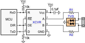
To protect bus nodes against high-energy transients, the implementation of external transient protection devices is therefore necessary. Figure 25 shows a protection circuit against 10-kV ESD (IEC 61000-4-2), 4-kV EFT (IEC 61000-4-4), and 1-kV surge (IEC 61000-4-5) transients.
 Figure 25. Transient Protection Against ESD, EFT, and Surge Transients
Table 4. Bill of Materials
| DEVICE | FUNCTION | ORDER NUMBER | MANUFACTURER |
|---|---|---|---|
| XCVR | 3.3-V, full-duplex RS-485 transceiver | SN65HVD11-HT | TI |
| R1, R2 | 10-Ω, pulse-proof, thick-film resistor | CRCW0603010RJNEAHP | Vishay |
| TVS | Bidirectional 400-W transient suppressor | CDSOT23-SM712 | Bourns |
9.2.3 Application Curve
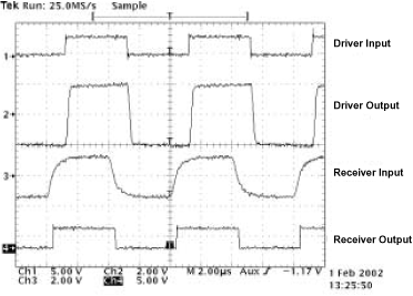
Figure 26 demonstrates operation of the SN65HVD11-HT at a signaling rate of 250 kbps. Two SN65HVD11-HT transceivers are used to transmit data through a 2000 foot (600 m) segment of Commscope 5524 category 5e+ twisted pair cable. The bus is terminated at each end by a 100-Ω resistor, matching the cable characteristic impedance.
 Figure 26. SN65HVD11-HT Input and Output Through 2000 Feet of Cable