SLLSE49D September 2010 – July 2017 SN65HVD1780-Q1 , SN65HVD1781-Q1 , SN65HVD1782-Q1
UNLESS OTHERWISE NOTED, this document contains PRODUCTION DATA.
- 1 Features
- 2 Applications
- 3 Description
- 4 Revision History
- 5 Pin Configuration and Functions
- 6 Specifications
- 7 Parameter Measurement Information
- 8 Detailed Description
- 9 Application and Implementation
- 10Power Supply Recommendations
- 11Layout
- 12Device and Documentation Support
- 13Mechanical, Packaging, and Orderable Information
Package Options
Mechanical Data (Package|Pins)
- D|8
Thermal pad, mechanical data (Package|Pins)
Orderable Information
6 Specifications
6.1 Absolute Maximum Ratings
See Note (1).| MIN | MAX | UNIT | |||||
|---|---|---|---|---|---|---|---|
| VCC | Supply voltage | –0.5 | 7 | V | |||
| Voltage range at bus pins | 'HVD1780-Q1, 'HVD1781-Q1 | A, B pins | –70 | 70 | V | ||
| 'HVD1782-Q1 | A, B pins | –70 | 30 | ||||
| Input voltage range at any logic pin | –0.3 | VCC + 0.3 | V | ||||
| Transient overvoltage pulse through 100 Ω per TIA-485 | –70 | 70 | V | ||||
| Receiver output current | –24 | 24 | mA | ||||
| Continuous total power dissipation | See Power Dissipation Ratings | ||||||
| TJ | Junction temperature | 170 | °C | ||||
| Tstg | Storage temperature | –40 | 150 | °C | |||
(1) Stresses beyond those listed under Absolute Maximum Ratings may cause permanent damage to the device. These are stress ratings only and functional operation of the device at these or any other conditions beyond those indicated under Recommended Operating Conditions is not implied. Exposure to absolute-maximum-rated conditions for extended periods may affect device reliability.
6.2 ESD Ratings—AEC
| VALUE | UNIT | |||||
|---|---|---|---|---|---|---|
| V(ESD) | Electrostatic discharge | Human-body model (HBM), per AEC Q100-002(1) | Bus terminals and GND | ±16000 | V | |
| All pins | ±4000 | |||||
| Charged-device model (CDM), per AEC Q100-011 | ±2000 | |||||
| Machine Model (MM), AEC-Q100-003 | ±400 | |||||
(1) AEC Q100-002 indicates that HBM stressing shall be in accordance with the ANSI/ESDA/JEDEC JS-001 specification.
6.3 ESD Ratings—IEC
| VALUE | UNIT | |||||
|---|---|---|---|---|---|---|
| V(ESD) | Electrostatic discharge | Human body model (HBM), per IEC 60749-26 | Bus terminals and GND | ±16000 | V | |
6.4 Recommended Operating Conditions
| MIN | NOM | MAX | UNIT | |||
|---|---|---|---|---|---|---|
| VCC | Supply voltage | 3.15 | 5 | 5.5 | V | |
| VI | Input voltage at any bus terminal (separately or common mode)(1) | –7 | 12 | V | ||
| VIH | High-level input voltage (driver, driver enable, and receiver enable inputs) | 2 | VCC | V | ||
| VIL | Low-level input voltage (driver, driver enable, and receiver enable inputs) | 0 | 0.8 | V | ||
| VID | Differential input voltage | –12 | 12 | V | ||
| IO | Output current, driver | –60 | 60 | mA | ||
| Output current, receiver | –8 | 8 | mA | |||
| RL | Differential load resistance | 54 | 60 | Ω | ||
| CL | Differential load capacitance | 50 | pF | |||
| 1/tUI | Signaling rate | SN65HVD1780-Q1 | 0.115 | Mbps | ||
| SN65HVD1781-Q1 | 1 | |||||
| SN65HVD1782-Q1 | 10 | |||||
| TA | Operating free-air temperature (See the Thermal Information table) | 5-V supply | –40 | 105 | °C | |
| 3.3-V supply | –40 | 125 | ||||
| TJ | Junction Temperature | –40 | 150 | °C | ||
(1) By convention, the least positive (most negative) limit is designated as minimum in this data sheet.
6.5 Thermal Information
| THERMAL METRIC(1) | SN65HVD1780-Q1 SN65HVD1781-Q1 SN65HVD1782-Q1 |
UNIT | ||
|---|---|---|---|---|
| D (SOIC) | ||||
| 8 PINS | ||||
| RθJA | Junction-to-ambient thermal resistance | JEDEC high-K model | 138 | °C/W |
| JEDIC low-K model | 242 | °C/W | ||
| RθJC(top) | Junction-to-case (top) thermal resistance | 61 | °C/W | |
| RθJB | Junction-to-board thermal resistance | 62 | °C/W | |
| ψJT | Junction-to-top characterization parameter | 3.8 | °C/W | |
| ψJB | Junction-to-board characterization parameter | 38.6 | °C/W | |
| RθJC(bot) | Junction-to-case (bottom) thermal resistance | N/A | °C/W | |
(1) For more information about traditional and new thermal metrics, see the Semiconductor and IC Package Thermal Metrics application report, SPRA953.
6.6 Electrical Characteristics
over recommended operating conditions (unless otherwise noted)| PARAMETER | TEST CONDITIONS | MIN | TYP | MAX | UNIT | |||
|---|---|---|---|---|---|---|---|---|
| |VOD| | Driver differential output voltage magnitude | RL = 60 Ω, 4.75 V ≤ VCC 375 Ω on each output to –7 V to 12 V, SeeFigure 6 |
TA < 85°C | 1.5 | V | |||
| TA < 125°C | 1.4 | |||||||
| RL = 54 Ω, 4.75 V ≤ VCC ≤ 5.25 V |
TA < 85°C | 1.7 | 2 | |||||
| TA < 125°C | 1.5 | |||||||
| RL = 54 Ω, 3.15 V ≤ VCC ≤ 3.45 V |
0.8 | 1 | ||||||
| RL = 100 Ω, 4.75 V ≤ VCC ≤ 5.25 V |
TA < 85°C | 2.2 | 2.5 | |||||
| TA < 125°C | 2 | |||||||
| Δ|VOD| | Change in magnitude of driver differential output voltage | RL = 54 Ω | –50 | 0 | 50 | mV | ||
| VOC(SS) | Steady-state common-mode output voltage | 1 | VCC/2 | 3 | V | |||
| ΔVOC | Change in differential driver output common-mode voltage | –50 | 0 | 50 | mV | |||
| VOC(PP) | Peak-to-peak driver common-mode output voltage | Center of two 27-Ω load resistors, See Figure 7 |
500 | mV | ||||
| COD | Differential output capacitance | 23 | pF | |||||
| VIT+ | Positive-going receiver differential input voltage threshold | –100 | –35 | mV | ||||
| VIT– | Negative-going receiver differential input voltage threshold | –180 | –150 | mV | ||||
| VHYS | Receiver differential input voltage threshold hysteresis (VIT+ – VIT–)(1) |
30 | 50 | mV | ||||
| VOH | Receiver high-level output voltage | IOH = –8 mA | 2.4 | VCC – 0.3 | V | |||
| VOL | Receiver low-level output voltage | IOL = 8 mA | TA < 85°C | 0.2 | 0.4 | V | ||
| TA < 125°C | 0.5 | |||||||
| II(LOGIC) | Driver input, driver enable, and receiver enable input current | –50 | 50 | μA | ||||
| IOZ | Receiver output high-impedance current | VO = 0 V or VCC, RE at VCC | –1 | 1 | μA | |||
| IOS | Driver short-circuit output current | –200 | 200 | mA | ||||
| II(BUS) | Bus input current (disabled driver) | VCC = 3.15 to 5.5 V or VCC = 0 V, DE at 0 V |
VI = 12 V | HVD1780-Q1, HVD1781-Q1 | 75 | 100 | μA | |
| HVD1782-Q1 | 400 | 500 | ||||||
| VI = –7 V | HVD1780-Q1, HVD1781-Q1 | –60 | –40 | |||||
| HVD1782-Q1 | -400 | -300 | ||||||
| ICC | Supply current (quiescent) | Driver and receiver enabled | DE = VCC, RE = GND, no load |
4 | 6 | mA | ||
| Driver enabled, receiver disabled | DE = VCC, RE = VCC, no load |
3 | 5 | |||||
| Driver disabled, receiver enabled | DE = GND, RE = GND, no load |
2 | 4 | |||||
| Driver and receiver disabled, standby mode | DE = GND, D = open, RE = VCC, no load, TA < 85°C |
0.15 | 1 | μA | ||||
| DE = GND, D = open, RE = VCC, no load, TA < 125°C |
12 | |||||||
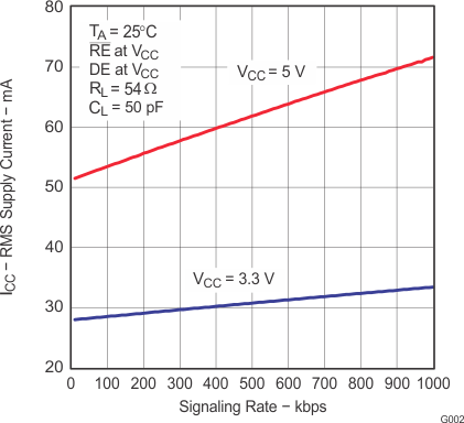
| Supply current (dynamic) | See the Typical Characteristics section | |||||||
(1) Ensured by design. Not production tested.
6.7 Power Dissipation Ratings
| PARAMETER | TEST CONDITIONS | VALUE | UNIT | |||
|---|---|---|---|---|---|---|
| PD | Power dissipation | VCC = 3.6 V, TJ = 150°C, RL = 300 Ω, CL = 50 pF (driver), CL = 15 pF (receiver) 3.3-V supply, unterminated(1) |
75 | mW | ||
| VCC = 3.6 V, TJ = 150°C, RL = 100 Ω, CL = 50 pF (driver), CL = 15 pF (receiver) 3.3-V supply, RS-422 load(1) |
95 | |||||
| VCC = 3.6 V, TJ = 150°C, RL = 54 Ω, CL = 50 pF (driver), CL = 15 pF (receiver) 3.3-V supply, RS-485 load(1) |
115 | |||||
| VCC = 5.5 V, TJ = 150°C, RL = 300 Ω, CL = 50 pF (driver), CL = 15 pF (receiver) 5-V supply, unterminated(1) |
290 | |||||
| VCC = 5.5 V, TJ = 150°C, RL = 100 Ω, CL = 50 pF (driver), CL = 15 pF (receiver) 5-V supply, RS-422 load(1) |
320 | |||||
| VCC = 5.5 V, TJ = 150°C, RL = 54 Ω, CL = 50 pF (driver), CL = 15 pF (receiver) 5-V supply, RS-485 load(1) |
400 | |||||
| TSD | Thermal-shutdown junction temperature | 170 | °C | |||
(1) Driver and receiver enabled, 50% duty cycle square-wave signal at signaling rate: 1 Mbps.
6.8 Switching Characteristics
over recommended operating conditions (unless otherwise noted)| PARAMETER | TEST CONDITIONS | MIN | TYP | MAX | UNIT | ||
|---|---|---|---|---|---|---|---|
| DRIVER (SN65HVD1780) | |||||||
| tr, tf | Driver differential output rise/fall time | RL = 54 Ω, CL = 50 pF, See Figure 8 |
3.15 V < VCC < 3.45 V | 0.4 | 1.4 | 1.8 | μs |
| 3.15 V < VCC < 5.5 V | 0.4 | 1.7 | 2.6 | µs | |||
| tPHL, tPLH | Driver propagation delay | RL = 54 Ω, CL = 50 pF, See Figure 8 | 0.8 | 2 | μs | ||
| tSK(P) | Driver differential output pulse skew, |tPHL – tPLH| |
RL = 54 Ω, CL = 50 pF, See Figure 8 | 20 | 250 | ns | ||
| tPHZ, tPLZ | Driver disable time | See Figure 9 and Figure 10 | 0.1 | 5 | μs | ||
| tPZH, tPZL | Driver enable time | Receiver enabled | See Figure 9 and Figure 10 | 0.2 | 3 | μs | |
| Receiver disabled | 3 | 12 | |||||
| DRIVER (SN65HVD1781) | |||||||
| tr, tf | Driver differential output rise/fall time | RL = 54 Ω, CL = 50 pF, See Figure 8 | 50 | 300 | ns | ||
| tPHL, tPLH | Driver propagation delay | RL = 54 Ω, CL = 50 pF, See Figure 8 | 200 | ns | |||
| tSK(P) | Driver differential output pulse skew, |tPHL – tPLH| |
RL = 54 Ω, CL = 50 pF, See Figure 8 | 25 | ns | |||
| tPHZ, tPLZ | Driver disable time | See Figure 9 and Figure 10 | 3 | μs | |||
| tPZH, tPZL | Driver enable time | Receiver enabled | See Figure 9 and Figure 10 | 300 | ns | ||
| Receiver disabled | 10 | μs | |||||
| DRIVER (SN65HVD1782) | |||||||
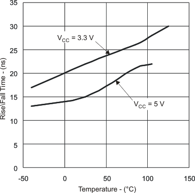
| tr, tf | Driver differential output rise/fall time | RL = 54 Ω, CL = 50 pF |
All VCC and Temp | 50 | ns | ||
| VCC > 4.5V and T < 105°C | 16 | ||||||
| tPHL, tPLH | Driver propagation delay | RL = 54 Ω, CL = 50 pF, See Figure 8 | 55 | ns | |||
| tSK(P) | Driver differential output pulse skew, |tPHL – tPLH| |
RL = 54 Ω, CL = 50 pF, See Figure 8 | 10 | ns | |||
| tPHZ, tPLZ | Driver disable time | See Figure 9 and Figure 10 | 3 | μs | |||
| tPZH, tPZL | Driver enable time | Receiver enabled | See Figure 9 and Figure 10 | 300 | ns | ||
| Receiver disabled | 9 | μs | |||||
| RECEIVER (ALL DEVICES UNLESS OTHERWISE NOTED) | |||||||
| tr, tf | Receiver output rise/fall time (1) | CL = 15 pF, See Figure 11 |
All devices | 4 | 15 | ns | |
| tPHL, tPLH | Receiver propagation delay time | CL = 15 pF, See Figure 11 |
HVD1780-Q1, HVD1781-Q1 |
100 | 200 | ns | |
| HVD1782-Q1 | 80 | ||||||
| tSK(P) | Receiver output pulse skew, |tPHL – tPLH| |
CL = 15 pF, See Figure 11 |
HVD1780-Q1, HVD1781-Q1 |
6 | 20 | ns | |
| HVD1782-Q1 | 5 | ||||||
| tPLZ, tPHZ | Receiver disable time (1) | Driver enabled, See Figure 12 | 15 | 100 | ns | ||
| tPZL(1), tPZH(1)
tPZL(2), tPZH(2) |
Receiver enable time | Driver enabled, See Figure 12 | 80 | 300 | ns | ||
| Driver disabled, See Figure 13 | 3 | 9 | μs | ||||
(1) Ensured by design. Not production tested.
6.9 Package Dissipation Ratings
| PACKAGE(1) | JEDEC THERMAL MODEL | TA < 25°C RATING |
DERATING FACTOR ABOVE TA = 25°C |
TA = 85°C RATING |
TA = 105°C RATING |
TA = 125°C RATING (3.3 V ONLY) |
|---|---|---|---|---|---|---|
| SOIC (D) 8-pin | High-K | 905 mW | 7.25 mW/°C | 470 mW | 325 mW | 180 mW |
| Low-K | 516 mW | 4.1 mW/°C | 268 mW | 186 mW | 103 mW |
(1) For the most current package and ordering information, see the Mechanical, Packaging, and Orderable Information section, or see the TI website at www.ti.com.
