SLLSF08A May 2017 – February 2022 SN65HVD1781A-Q1
PRODUCTION DATA
- 1 Features
- 2 Applications
- 3 Description
- 4 Revision History
- 5 Pin Configuration and Functions
- 6 Specifications
- 7 Parameter Measurement Information
- 8 Detailed Description
- 9 Application and Implementation
- 10Power Supply Recommendations
- 11Layout
- 12Device and Documentation Support
- 13Mechanical, Packaging, and Orderable Information
Package Options
Mechanical Data (Package|Pins)
- D|8
Thermal pad, mechanical data (Package|Pins)
Orderable Information
3 Description
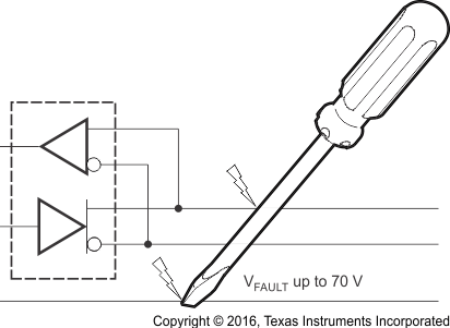
The device is designed to survive overvoltage faults such as direct shorts to power supplies, mis-wiring faults, connector failures, cable crushes, and tool mis-applications. It is also robust to ESD events, with high levels of protection to the human-body-model specification.
The SN65HVD1781A-Q1 combines a differential driver and a differential receiver, which operate from a single power supply. The driver differential outputs and the receiver differential inputs are connected internally to form a bus port suitable for half-duplex (two-wire bus) communication. This port features a wide common-mode voltage range, making the device suitable for multipoint applications over long cable runs. The device is characterized from –40°C to 125°C. The SN65HVD1781A-Q1 device is pin-compatible with the industry-standard SN75176 transceiver, making it a drop-in upgrade in most systems.
The device is fully compliant with ANSI TIA/EIA 485-A with a 5-V supply and can operate with a 3.3-V supply with reduced driver output voltage for low-power applications. For applications where operation is required over an extended common-mode voltage range, see the SN65HVD1785 (SLLS872) data sheet.
| PART NUMBER | PACKAGE(1) | BODY SIZE (NOM) |
|---|---|---|
| SN65HVD1781A-Q1 | SOIC | 4.90 mm x 3.91 mm |
 Simplified Schematic