SLLS552G December 2002 – September 2022 SN65HVD20 , SN65HVD21 , SN65HVD22 , SN65HVD23 , SN65HVD24
PRODUCTION DATA
- 1 Features
- 2 Applications
- 3 Description
- 4 Revision History
- 5 Description (continued)
- 6 Device Comparison
- 7 Pin Configuration and Functions
-
8 Specifications
- 8.1 Absolute Maximum Ratings
- 8.2 ESD Ratings
- 8.3 Recommended Operating Conditions
- 8.4 Thermal Information
- 8.5 Driver Electrical Characteristics
- 8.6 Receiver Electrical Characteristics
- 8.7 Driver Switching Characteristics
- 8.8 Receiver Switching Characteristics
- 8.9 Receiver Equalization Characteristics
- 8.10 Power Dissipation
- 8.11 Typical Characteristics
- 9 Parameter Measurement Information
- 10Detailed Description
- 11Application and Implementation
- 12Power Supply Recommendations
- 13Layout
- 14Device and Documentation Support
- 15Mechanical, Packaging, and Orderable Information
Package Options
Mechanical Data (Package|Pins)
Thermal pad, mechanical data (Package|Pins)
Orderable Information
3 Description
The transceivers in the SN65HVD2x family offer performance far exceeding typical RS-485 devices. In addition to meeting all requirements of the TIA/EIA‑485-A standard. The SN65HVD2x family operates over an extended range of common-mode voltages and has features such as high ESD protection, wide receiver hysteresis, and failsafe operation. This family of devices is designed for long-cable networks, and other applications where the environment is too harsh for ordinary transceivers.
These devices are designed for bidirectional data transmission on multipoint twisted-pair cables. Example applications are digital motor controllers, remote sensors and terminals, industrial process control, security stations, and environmental control systems.
These devices combine a 3-state differential driver and a differential receiver that operate from a single 5-V power supply. The driver differential outputs and the receiver differential inputs are connected internally to form a differential bus port that offers minimum loading to the bus. This port features an extended common-mode voltage range, making the device suitable for multipoint applications over long cable runs.
| PART NUMBER | PACKAGE(1) | BODY SIZE (NOM) |
|---|---|---|
| SN65HVD2x | SOIC (8) | 4.90 mm × 3.91 mm |
| PDIP (8) | 9.81 mm × 6.35 mm |
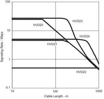
 SN65HVD2x Application
Space
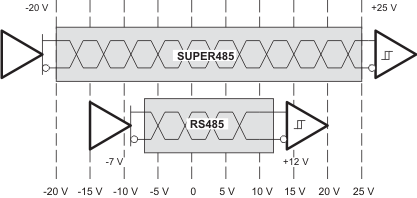
 SN65HVD2x Devices Operate
Over a Wider Common-Mode Voltage Range