SLASEE6 September 2016 SN65HVS883
PRODUCTION DATA.
- 1 Features
- 2 Applications
- 3 Description
- 4 Revision History
- 5 Pin Configuration and Functions
- 6 Specifications
- 7 Parameter Measurement Information
- 8 Detailed Description
- 9 Application and Implementation
- 10Power Supply Recommendations
- 11Layout
- 12Device and Documentation Support
- 13Mechanical, Packaging, and Orderable Information
Package Options
Mechanical Data (Package|Pins)
- PWP|28
Thermal pad, mechanical data (Package|Pins)
- PWP|28
Orderable Information
8 Detailed Description
8.1 Overview
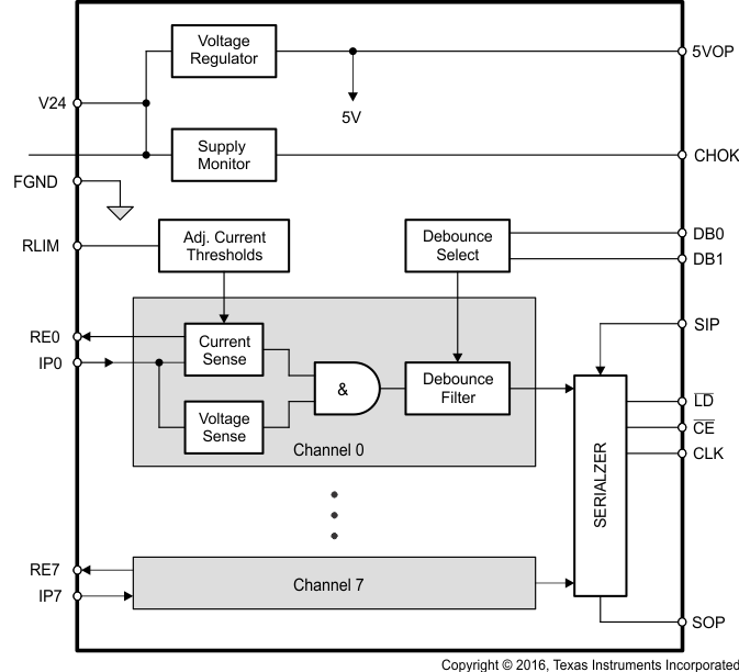
The SN65HVS883 is an 8 channel, digital input serializer which operates from a 24 V supply and accepts digital inputs of up to 34 V on the 8 channels (IP0-IP7). The device provides a serially shifted digital output with reduced voltage ranges of 0-5 V for applications in industrial and building automation systems. The SN65HVS883 meets JEDEC standards for ESD protection (refer to ESD Ratings), and is SPI compatible for interfacing with standard microcontrollers. The serializer operates in 2 fundamental modes: Load Mode and Shift mode. In Load mode, information from the field inputs is allowed to latch into the shift register. In Shift mode, the information stored in the parallel shift register can be serially shifted to the serial output (SOP). A detailed description of the functional modes is available in the Device Functional Modes section.
8.2 Functional Block Diagram

8.3 Feature Description
8.3.1 Digital Inputs
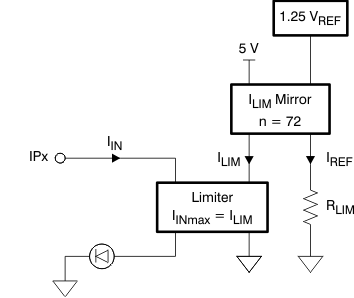
Each digital input operates as a controlled current sink limiting the input current to a maximum value of ILIM. The current limit is derived from the reference current via ILIM = n × IREF, and IREF is determined by IREF = VREF/RLIM. Thus, changing the current limit requires the change of RLIM to a different value via: RLIM = n × VREF/ILIM.
Inserting the actual values for n and VREF gives: RLIM = 90 V / ILIM.
While the device is specified for a current limit of 3.6 mA, (via RLIM = 25 kΩ), it is easy to lower the current limit to further reduce the power consumption. For example, for a current limit of 2.5 mA simply calculate:

 Figure 13. Digital Input Stage
8.3.2 Debounce Filter
The HVS883 applies a simple analog/digital filtering technique to remove unintended signal transitions due to contact bounce or other mechanical effects. Any new input (either low or high) must be present for the duration of the selected debounce time to be latched into the shift register as a valid state.
The logic signal levels at the control inputs, DB0 and DB1 of the internal Debounce-Select logic determine the different debounce times listed in the following truth table.
Table 1. Debounce Times
| DB1 | DB0 | FUNCTION | |
|---|---|---|---|
| Open | Open | 3 ms delay | |
| Open | FGND | 1 ms delay | |
| FGND | Open | 0 ms delay (Filter bypassed) |
|
| FGND | FGND | Reserved |
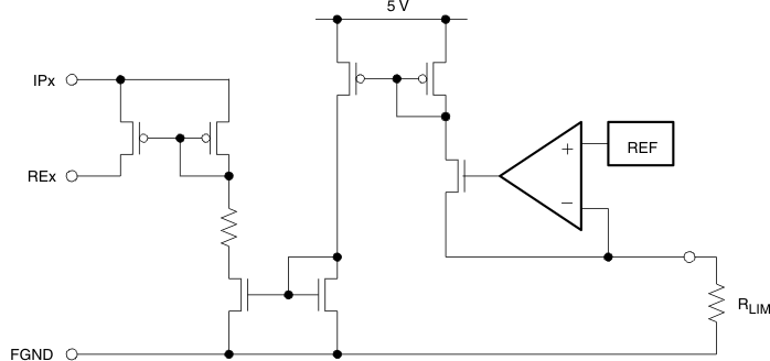
 Figure 14. Equivalent Input Diagram
8.3.3 Shift Register
The conversion from parallel input to serial output data is performed by an eight-channel, parallel-in serial-out shift register. Parallel-in access is provided by the internal inputs, PIP0–PIP7, that are enabled by a low level at the load input (LD). When clocked, the latched input data shift towards the serial output (SOP). The shift register also provides a clock-enable function.
Clocking is accomplished by a low-to-high transition of the clock (CLK) input while LD is held high and the clock enable (CE) input is held low for all registers in the shift register except the last register which is latched by a high-to-low transition. Parallel loading is inhibited when LD is held high. The parallel inputs to the register are enabled while LD is low independently of the levels of the CLK, CE, or serial (SIP) inputs.
 Figure 15. Shift Register Logic Structure
8.3.4 Voltage Regulator
The on-chip linear voltage regulator provides a 5 V supply to the internal- and external circuitry, such as digital isolators, with an output drive capability of 50 mA and a typical current limit of 115 mA. The regulator accepts input voltages from 34 V down to 10 V. Because the regulator output is intended to supply external digital isolator circuits proper output voltage decoupling is required. For best results connect a 1 μF and a 0.1 μF ceramic capacitor as close as possible to the 5VOP-output. For longer traces between the SN65HVS883 and isolators of the ISO72xx family use additional 0.1 μF and 10 pF capacitors next to the isolator supply pins. Make sure, however, that the total load capacitance does not exceed 4.7 μF.
For good stability the voltage regulator requires a minimum load current, IL-MIN. Ensure that under any operating condition the ratio of the minimum load current in mA to the total load capacitance in μF is larger than 1:

8.3.5 Supply Voltage Monitor
The integrated supply voltage monitor senses the supply voltage of the SN65HVS883 at the V24-pin. If this voltage drops below 15 V but stays within the regulator’s operating range, i.e., 15 V > V24 > 10 V, the output CHOK goes low 1 ms later. When the supply voltage returns to 24 V, the CHOK output turns logic high after
6 ms. Should the supply voltage drop below 10 V, the device ceases operation. Upon the supply returning to above 18 V, the CHOK output turns high again after 6 ms.
 Figure 16. CHOK Output Timing as a Function of Supply Voltage Drop at V24
8.4 Device Functional Modes
The 2 functional modes of operation are Load mode and Shift mode.
Load mode enables information from the field inputs to latch into the shift register. To enter load mode, the LD pin must be held low, and the device remains in load mode regardless of the CLK, CE, or serial (SIP) input levels. A high level at the LD pin switches the device into Shift mode.
When the device is in Shift mode, a low level at the CE pin causes the data stored in all registers of the parallel shift register except for the last register, to be serially shifted toward the serial output (SOP) on the rising edge of CLK. The final register in the shift register will be shifted toward the serial output (SOP) on the falling edge of CLK. A high level at the CE pin inhibits the serial shifting, which is demonstrated in Figure 21. After 8 consecutive CLK cycles, the serial output (SOP) remains at the level of the serial input (SIP) which is internally pulled to logic high. A logic high at the CE pin is required to signify the end of the serial data output. For of a daisy chained configuration, the serial output (SOP) of the SN65HVS883 can be connected to the serial input (SIP) of a following device, and additional clock cycles are required to shift the additional data out of the chain. The number of consecutive clock cycles will equal 8 times the number of devices in the chain. See Figure 22 for an example of a cascaded chain of 4x SN65HVS883.