SLLS174I February 1994 – October 2022 SN55LBC180 , SN65LBC180 , SN75LBC180
PRODUCTION DATA
- 1 Features
- 2 Description
- 3 Description (Continued)
- 4 Revision History
- 5 Pin Configuration and Functions
- 6 Specifications
- 7 Parameter Measurement Information
- 8 Detailed Description
- 9 Application and Implementation
- 10Device and Documentation Support
- 11Mechanical, Packaging, and Orderable Information
Package Options
Refer to the PDF data sheet for device specific package drawings
Mechanical Data (Package|Pins)
- D|14
- RSA|16
- N|14
Thermal pad, mechanical data (Package|Pins)
Orderable Information
2 Description
The SN55LBC180, SN65LBC180 and SN75LBC180 differential driver and receiver pairs are monolithic integrated circuits designed for bidirectional data communication over long cables that take on the characteristics of transmission lines. They are balanced, or differential, voltage mode devices that meet or exceed the requirements of industry standards ANSI RS-485 and ISO 8482:1987(E). These devices are designed using the TI proprietary LinBiCMOS™ with the low-power consumption of CMOS and the precision and robustness of bipolar transistors in the same circuit.
| PART NUMBER | PACKAGE(1) | BODY SIZE (NOM) |
|---|---|---|
|
SN75LBC180 SN65LBC180 |
N (PDIP) | 19.3 mm x 63.5 mm |
| D (SOIC) | 8.65 mm x 3.91 mm | |
| RSA (QFN) | 4 mm x 4 mm | |
| SN55LBC180 | RSA (QFN) | 4 mm x 4 mm |
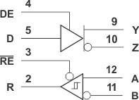
 Logic Diagram (positive logic)