SCLS258M December 1995 – April 2024 SN54AHC138 , SN74AHC138
PRODUCTION DATA
- 1
- 1 Features
- 2 Description
- 3 Pin Configuration and Functions
- 4 Specifications
- 5 Parameter Measurement Information
- 6 Detailed Description
- 7 Application and Implementation
- 8 Device and Documentation Support
- 9 Revision History
- 10Mechanical, Packaging, and Orderable Information
Package Options
Refer to the PDF data sheet for device specific package drawings
Mechanical Data (Package|Pins)
- DB|16
- PW|16
- NS|16
- N|16
- RGY|16
- D|16
- DGV|16
Thermal pad, mechanical data (Package|Pins)
- RGY|16
Orderable Information
2 Description
The SNx4AHC138 decoders/demultiplexers are designed for high-performance memory-decoding and data-routing applications that require very short propagation-delay times. In high-performance memory systems, these decoders can be used to minimize the effects of system decoding. When employed with high-speed memories utilizing a fast enable circuit, the delay times of these decoders and the enable time of the memory usually are less than the typical access time of the memory. This means that the effective system delay introduced by the decoders is negligible.
| PART NUMBER | PACKAGE (1) | PACKAGE SIZE (2) | BODY SIZE (3) |
|---|---|---|---|
| SN74AHC138 | RGY (VQFN, 16) | 4mm x 3.5mm | 4mm x 3.5mm |
| N (PDIP, 16) | 19.3 mm × 9.4 mm | 19.32 mm x 6.35 mm | |
| D (SOIC, 16) | 9.9 mm × 6 mm | 9.90 mm x 3.90 mm | |
| NS (SOP, 16) | 10.2mm x 7.8mm | 10.20 mm x 5.30 mm | |
| DB (SSOP, 16) | 6.2 mm × 7.8 mm | 6.20 mm x 5.30 mm | |
| PW (TSSOP , 16) | 5 mm × 6.4 mm | 5.00 mm x 4.40 mm | |
| DGV (TVSOP, 16) | 3.6mm x 6.4mm | 3.6mm x 4.4mm |
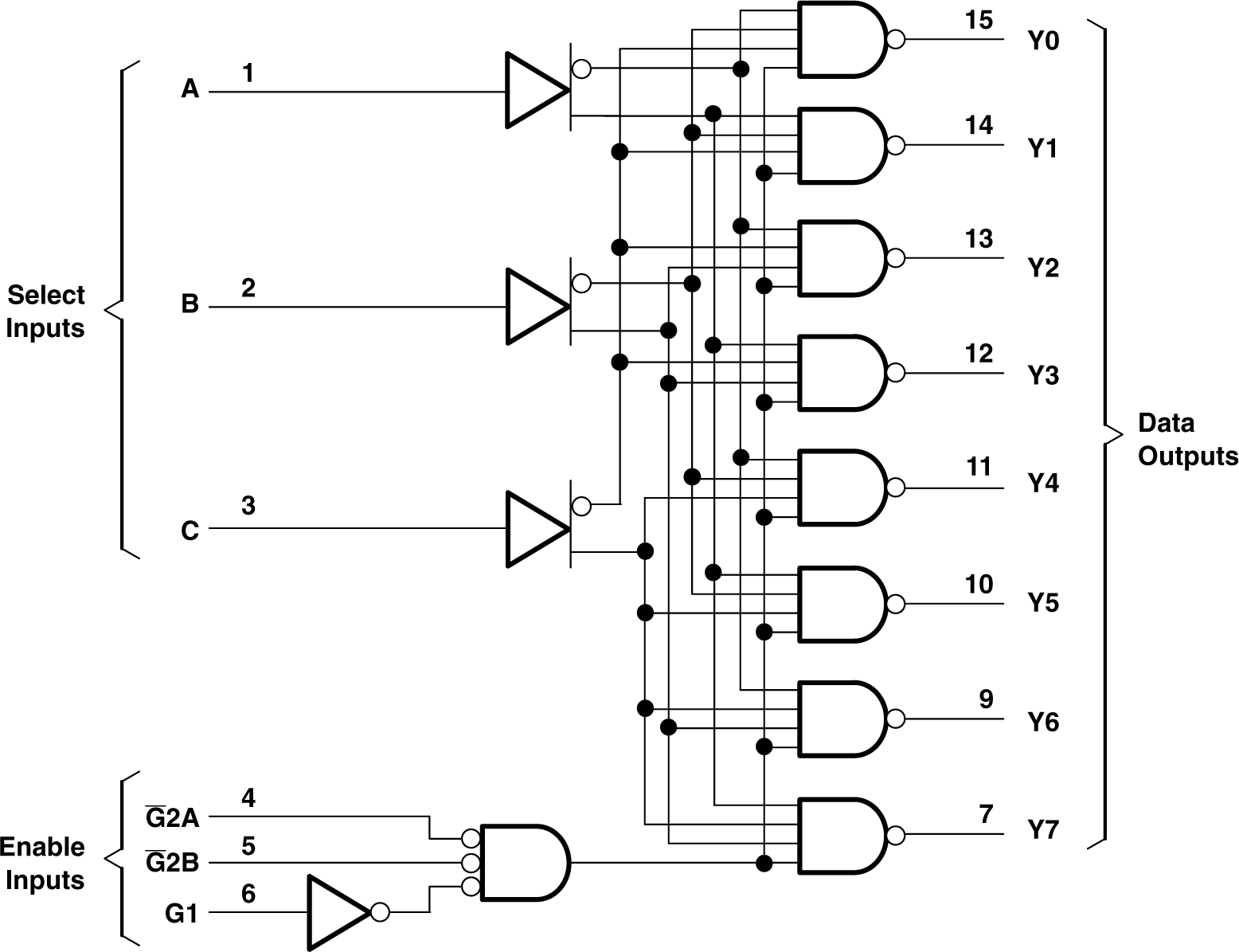
 Logic Diagram (Positive Logic)