SCLS255N December 1995 – February 2024 SN54AHC74 , SN74AHC74
PRODUCTION DATA
- 1
- 1 Features
- 2 Applications
- 3 Description
- 4 Pin Configuration and Functions
-
5 Specifications
- 5.1 Absolute Maximum Ratings
- 5.2 ESD Ratings
- 5.3 Recommended Operating Conditions
- 5.4 Thermal Information — SN74AHC74
- 5.5 Electrical Characteristics
- 5.6 Timing Requirements — VCC = 3.3 V ± 0.3 V
- 5.7 Timing Requirements — VCC = 5 V ± 0.5 V
- 5.8 Switching Characteristics — VCC = 3.3 V ± 0.5 V
- 5.9 Switching Characteristics — VCC = 5 V ± 0.5 V
- 5.10 Noise Characteristics
- 5.11 Operating Characteristics
- 6 Parameter Measurement Information
- 7 Detailed Description
- 8 Application and Implementation
- 9 Device and Documentation Support
- 10Revision History
- 11Mechanical, Packaging, and Orderable Information
Package Options
Refer to the PDF data sheet for device specific package drawings
Mechanical Data (Package|Pins)
- D|14
- RGY|14
- DB|14
- DGV|14
- PW|14
- BQA|14
- N|14
- NS|14
Thermal pad, mechanical data (Package|Pins)
Orderable Information
3 Description
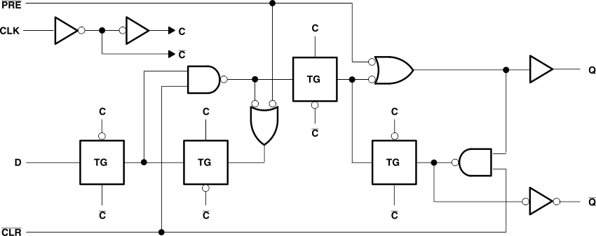
The SNx4AHC74 dual positive-edge-triggered devices are D-type flip-flops.
A low level at the preset (PRE) or clear (CLR) inputs sets or resets the outputs, regardless of the levels of the other inputs. When PRE and CLR are inactive (high), data at the data (D) input meeting the setup time requirements is transferred to the outputs on the positive-going edge of the clock pulse. Clock triggering occurs at a voltage level and is not directly related to the rise time of the clock pulse. Following the hold-time interval, data at the D input can be changed without affecting the levels at the outputs.
| PART NUMBER | RATING | PACKAGE(1) |
|---|---|---|
| SN54AHC74 | Military | FK (LCCC, 20) |
| J (CDIP, 14) | ||
| W (CFP, 14) | ||
| SN74AHC74 | Commercial | D (SOIC, 14) |
| DB (SSOP, 14) | ||
| DGV (TVSOP, 14) | ||
| N (PDIP, 14) | ||
| NS (SO, 14) | ||
| PW (TSSOP, 14) | ||
| RGY (VQFN, 14) | ||
BQA (WQFN, 14) |
 Logic Diagram (Positive Logic)