SCLS508C June 2003 – October 2023 SN74AHCT125-Q1
PRODUCTION DATA
- 1
- 1 Features
- 2 Applications
- 3 Description
- 4 Revision History
- 5 Pin Configuration and Functions
-
6 Specifications
- 6.1 Absolute Maximum Ratings
- 6.2 ESD Ratings
- 6.3 Recommended Operating Conditions
- 6.4 Thermal Information
- 6.5 Electrical Characteristics
- 6.6 Switching Characteristics
- 6.7 Noise Characteristics #GUID-59737337-6F0E-416E-BD36-E176D00EBAF4/SCLS5085302
- 6.8 Operating Characteristics
- 6.9 Typical Characteristics
- 7 Parameter Measurement Information
- 8 Detailed Description
- 9 Application and Implementation
- 10Device and Documentation Support
- 11Mechanical, Packaging, and Orderable Information
Package Options
Mechanical Data (Package|Pins)
Thermal pad, mechanical data (Package|Pins)
Orderable Information
5 Pin Configuration and Functions
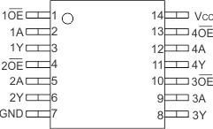
 Figure 5-1 D or PW Package, 14-pin SOIC or TSSOP(Top View)
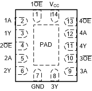
 Figure 5-2 BQA Package, 14-pin WQFN (Top View)
Table 5-1 Pin Functions
| PIN | TYPE(1) | DESCRIPTION | |
|---|---|---|---|
| NAME | NO. | ||
| 1 OE | 1 | I | Output enable |
| 1A | 2 | I | Input |
| 1Y | 3 | O | Output |
| 2 OE | 4 | I | Output enable |
| 2A | 5 | I | Input |
| 2Y | 6 | O | Output |
| 3 OE | 8 | I | Output enable |
| 3A | 9 | I | Input |
| 3Y | 10 | I | Output |
| 4 OE | 13 | I | Output enable |
| 4A | 12 | I | Input |
| 4Y | 11 | O | Output |
| GND | 7 | – | Ground |
| VCC | 14 | I | Supply voltage |
(1) I = input, O = output