SCLS375F June 1997 – July 2014 SN74AHCT273
PRODUCTION DATA.
- 1 Features
- 2 Applications
- 3 Description
- 4 Simplified Schematics
- 5 Revision History
- 6 Pin Configuration and Functions
- 7 Specifications
- 8 Parameter Measurement Information
- 9 Detailed Description
- 10Application and Implementation
- 11Power Supply Recommendations
- 12Layout
- 13Device and Documentation Support
- 14Mechanical, Packaging, and Orderable Information
Package Options
Refer to the PDF data sheet for device specific package drawings
Mechanical Data (Package|Pins)
- DB|20
- NS|20
- N|20
- DW|20
- PW|20
Thermal pad, mechanical data (Package|Pins)
Orderable Information
9 Detailed Description
9.1 Overview
These circuits are positive-edge-triggered D-type flip-flops with a direct clear (CLR) input. Information at the data (D) inputs meeting the setup time requirements is transferred to the Q outputs on the positive-going edge of the clock (CLK) pulse. Clock triggering occurs at a particular voltage level and is not directly related to the transition time of the positive-going pulse. When CLK is at either the high or low level, the D input has no effect at the output.
The inputs are TTL compatible with VIL at 0.8 V and VIH at 2 V. This feature allows the use of these devices as up translators in a mixed 3.3 V to 5 V system environment.
9.2 Functional Block Diagrams
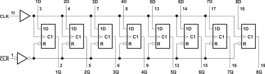 Figure 3. Logic Diagram (Positive Logic)
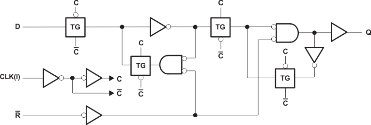 Figure 4. Logic Diagram, Each Flip-flop (Positive Logic)
9.3 Feature Description
- Allow up voltage translation from 3.3 V to 5 V
- Inputs accept TTL voltage levels
- Slow edge rates minimize output ringing
9.4 Device Functional Modes
Table 1. Function Table
(Each Flip-flop)
| INPUTS | OUTPUT Q |
||
|---|---|---|---|
| CLR | CLK | D | |
| L | X | X | L |
| H | ↑ | H | H |
| H | ↑ | L | L |
| H | L | X | Q0 |