SCDS008M May 1993 – June 2015 SN74CBT16214
PRODUCTION DATA.
- 1 Features
- 2 Applications
- 3 Description
- 4 Revision History
- 5 Pin Configuration and Functions
- 6 Specifications
- 7 Parameter Measurement Information
- 8 Detailed Description
- 9 Application and Implementation
- 10Power Supply Recommendations
- 11Layout
- 12Device and Documentation Support
- 13Mechanical, Packaging, and Orderable Information
Package Options
Refer to the PDF data sheet for device specific package drawings
Mechanical Data (Package|Pins)
- DGG|56
- DL|56
Thermal pad, mechanical data (Package|Pins)
Orderable Information
8 Detailed Description
8.1 Overview
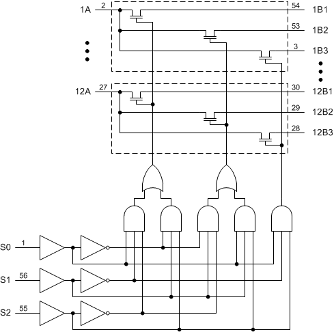
The SN74CBT16214 provides 12 bits of high-speed TTL-compatible bus switching between three separate ports. The low ON-state resistance of the switch allows connections to be made with minimal propagation delay.
The device operates as a 12-bit bus-select switch via the data-select (S0–S2) terminals.
8.2 Functional Block Diagram

8.3 Feature Description
The typical RON for each port is 5 Ω, reducing the amount of signal attenuation through the switch from higher impedance switches. Inputs operate with TTL-compatible voltages.
8.4 Device Functional Modes
Table 1 lists the functional modes for SN74CBT16214.
Table 1. Function Table
| INPUTS | INPUT/OUTPUT A |
FUNCTION | ||
|---|---|---|---|---|
| S2 | S1 | S0 | ||
| L | L | L | Z | Disconnect |
| L | L | H | B1 | A port = B1 port |
| L | H | L | B2 | A port = B2 port |
| L | H | H | Z | Disconnect |
| H | L | L | Z | Disconnect |
| H | L | H | B3 | A port = B3 port |
| H | H | L | B1 | A port = B1 port |
| H | H | H | B2 | A port = B2 port |