SCLS109H April 2004 – March 2022 SN54HC148 , SN74HC148
PRODUCTION DATA
- 1 Features
- 2 Applications
- 3 Description
- 4 Revision History
- 5 Pin Configuration and Functions
- 6 Specifications
- 7 Parameter Measurement Information
- 8 Detailed Description
- 9 Application Information
- 10Power Supply Recommendations
- 11Layout
- 12Device and Documentation Support
- 13Mechanical, Packaging, and Orderable Information
Package Options
Refer to the PDF data sheet for device specific package drawings
Mechanical Data (Package|Pins)
- NS|16
- N|16
- D|16
Thermal pad, mechanical data (Package|Pins)
- D|16
Orderable Information
9 Application Information
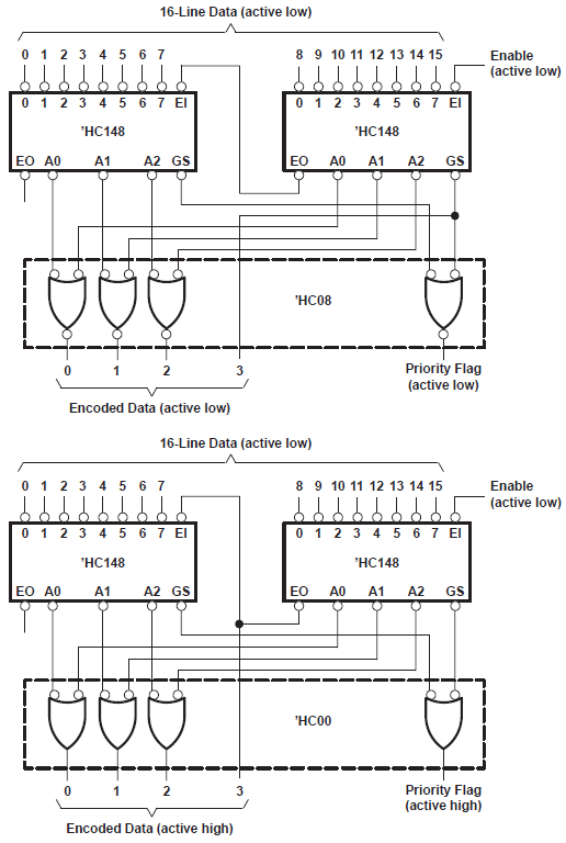
 Figure 9-1 Priority Encoder for 16 Bits
Because the ’HC148 devices are combinational logic circuits, wrong addresses can appear during input transients. Moreover, a change from high to low at EI can cause a transient low on GS when all inputs are high. This must be considered when strobing the outputs.