SCLS116H December 1982 – December 2015 SN54HC165 , SN74HC165
PRODUCTION DATA.
- 1 Features
- 2 Applications
- 3 Description
- 4 Revision History
- 5 Pin Configuration and Functions
-
6 Specifications
- 6.1 Absolute Maximum Ratings
- 6.2 ESD Ratings
- 6.3 Recommended Operating Conditions
- 6.4 Thermal Information
- 6.5 Electrical Characteristics, TA = 25°C
- 6.6 Electrical Characteristics, SN54HC165
- 6.7 Electrical Characteristics, SN74HC165
- 6.8 Switching Characteristics, TA = 25°C
- 6.9 Switching Characteristics, SN54HC165
- 6.10 Switching Characteristics, SN74HC165
- 6.11 Timing Requirements, TA = 25°C
- 6.12 Timing Requirements, SN54HC165
- 6.13 Timing Requirements, SN74HC165
- 6.14 Operating Characteristics
- 6.15 Typical Characteristics
- 7 Parameter Measurement Information
- 8 Detailed Description
- 9 Application and Implementation
- 10Power Supply Recommendations
- 11Layout
- 12Device and Documentation Support
- 13Mechanical, Packaging, and Orderable Information
Package Options
Refer to the PDF data sheet for device specific package drawings
Mechanical Data (Package|Pins)
- DB|16
- PW|16
- NS|16
- N|16
- D|16
Thermal pad, mechanical data (Package|Pins)
- D|16
Orderable Information
11 Layout
11.1 Layout Guidelines
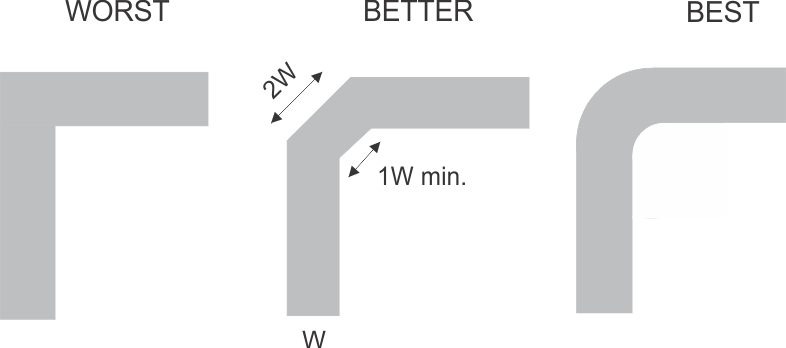
Reflections and matching are closely related to loop antenna theory, but different enough to warrant their own discussion. When a PCB trace turns a corner at a 90° angle, a reflection can occur. This is primarily due to the change of width of the trace. At the apex of the turn, the trace width is increased to 1.414 times its width. This upsets the transmission line characteristics, especially the distributed capacitance and self–inductance of the trace — resulting in the reflection. It is a given that not all PCB traces can be straight, and so they will have to turn corners. Figure 7 shows progressively better techniques of rounding corners. Only the last example maintains constant trace width and minimizes reflections.
11.2 Layout Example
 Figure 7. Trace Example