SDLS144D April 1985 – October 2016 SN54LS240 , SN54LS241 , SN54LS244 , SN54S240 , SN54S241 , SN54S244 , SN74LS240 , SN74LS241 , SN74LS244 , SN74S240 , SN74S241 , SN74S244
- 1 Features
- 2 Applications
- 3 Description
- 4 Revision History
- 5 Pin Configuration and Functions
-
6 Specifications
- 6.1 Absolute Maximum Ratings
- 6.2 ESD Ratings
- 6.3 Recommended Operating Conditions
- 6.4 Thermal Information
- 6.5 Electrical Characteristics - SNx4LS24x
- 6.6 Electrical Characteristics - SNx4S24x
- 6.7 Switching Characteristics - SNx4LS24x
- 6.8 Switching Characteristics - SNx4S24x
- 6.9 Typical Characteristics
- 7 Parameter Measurement Information
- 8 Detailed Description
- 9 Application and Implementation
- 10Power Supply Recommendations
- 11Layout
- 12Device and Documentation Support
- 13Mechanical, Packaging, and Orderable Information
Package Options
Mechanical Data (Package|Pins)
Thermal pad, mechanical data (Package|Pins)
Orderable Information
7 Parameter Measurement Information
7.1 SN54LS24x and SN74LS24x Devices
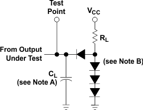 Figure 2. Load Circuit,
For 2-State Totem-Pole Outputs
 Figure 3. Load Circuit,
For Open-Collector Outputs
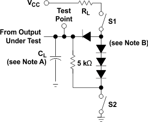 Figure 4. Load Circuit,
For 3-State Outputs
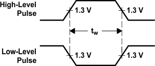 Figure 5. Voltage Waveforms,
Pulse Durations
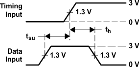 Figure 6. Voltage Waveforms,
Setup and Hold Times
 Figure 7. Voltage Waveforms,
Propagation Delay Times
A. CL includes probe and jig capacitance.
B. All diodes are 1N3064 or equivalent.
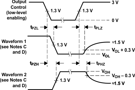
C. Waveform 1 is for an output with internal conditions such that the output is low except when disabled by the output control. Waveform 2 is for an output with internal conditions such that the output is high except when disabled by the output control.
D. S1 and S2 are closed for tPLH, tPHL, tPHZ, and tPLZ; S1 is open and S2 is closed for tPZH; S1 is closed and S2 is open for tPZL.
E. Phase relationships between inputs and outputs have been chosen arbitrarily for these examples.
F. All input pulses are supplied by generators having the following characteristics: PRR ≤ 1 MHz, ZO is approximately
50 Ω, tr ≤ 15 ns, tf ≤ 6 ns.
50 Ω, tr ≤ 15 ns, tf ≤ 6 ns.
G. The outputs are measured one at a time with one input transition per measurement.
Figure 8. Voltage Waveforms,Enable and Disable Times, 3-State Outputs
7.2 SN54S24x and SN74S24x Devices
 Figure 9. Load Circuit,
For 2-State Totem-Pole Outputs
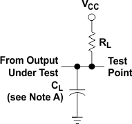 Figure 10. Load Circuit,
For Open-Collector Outputs
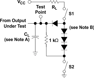 Figure 11. Load Circuit,
For 3-State Outputs
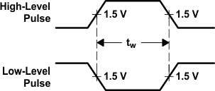 Figure 12. Voltage Waveforms,
Pulse Durations
 Figure 13. Voltage Waveforms,
Setup and Hold Times
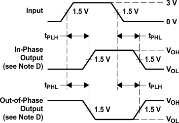 Figure 14. Voltage Waveforms,
Propagation Delay Times
A. CL includes probe and jig capacitance.
B. All diodes are 1N3064 or equivalent.
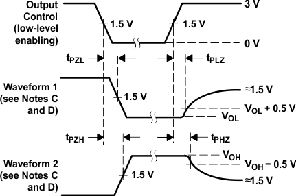
C. Waveform 1 is for an output with internal conditions such that the output is low except when disabled by the output control. Waveform 2 is for an output with internal conditions such that the output is high except when disabled by the output control.
D. S1 and S2 are closed for tPLH, tPHL, tPHZ, and tPLZ; S1 is open and S2 is closed for tPZH; S1 is closed and S2 is open for tPZL.
E. All input pulses are supplied by generators having the following characteristics: PRR ≤ 1 MHz, ZO is approximately
50 Ω; tr and tf ≤ 7 ns for SN54LS24x and SN74LS24x devices, and tr and tf ≤ 2.5 ns for SN54S24x and SN74S24x devices.
50 Ω; tr and tf ≤ 7 ns for SN54LS24x and SN74LS24x devices, and tr and tf ≤ 2.5 ns for SN54S24x and SN74S24x devices.
F. The outputs are measured one at a time with one input transition per measurement.
Figure 15. Voltage Waveforms,Enable and Disable Times, 3-State Outputs