SCES337K May 2000 – October 2014 SN74LV07A
PRODUCTION DATA.
- 1 Features
- 2 Applications
- 3 Description
- 4 Simplified Schematic
- 5 Revision History
- 6 Pin Configuration and Functions
-
7 Specifications
- 7.1 Absolute Maximum Ratings
- 7.2 Handling Ratings
- 7.3 Recommended Operating Conditions
- 7.4 Thermal Information
- 7.5 Electrical Characteristics
- 7.6 Switching Characteristics, VCC = 2.5 V ± 0.2 V
- 7.7 Switching Characteristics, VCC = 3.3 V ± 0.3 V
- 7.8 Switching Characteristics, VCC = 5 V ± 0.5 V
- 7.9 Noise Characteristics
- 7.10 Operating Characteristics
- 7.11 Typical Characteristics
- 8 Parameter Measurement Information
- 9 Detailed Description
- 10Application and Implementation
- 11Power Supply Recommendations
- 12Layout
- 13Device and Documentation Support
- 14Mechanical, Packaging, and Orderable Information
Package Options
Refer to the PDF data sheet for device specific package drawings
Mechanical Data (Package|Pins)
- D|14
- DB|14
- DGV|14
- PW|14
- NS|14
Thermal pad, mechanical data (Package|Pins)
- PW|14
Orderable Information
10 Application and Implementation
NOTE
Information in the following applications sections is not part of the TI component specification, and TI does not warrant its accuracy or completeness. TI’s customers are responsible for determining suitability of components for their purposes. Customers should validate and test their design implementation to confirm system functionality.
10.1 Application Information
The SN74LV07A device is a low drive, open-drain CMOS device that can be used for a multitude of buffer type functions. The inputs are 5.5-V tolerant. The outputs are open drain and 5.5-V tolerant; thus, allowing the device to translate up to 5.5 V or down to any other voltage between GND and 5.5 V.
10.2 Typical Application
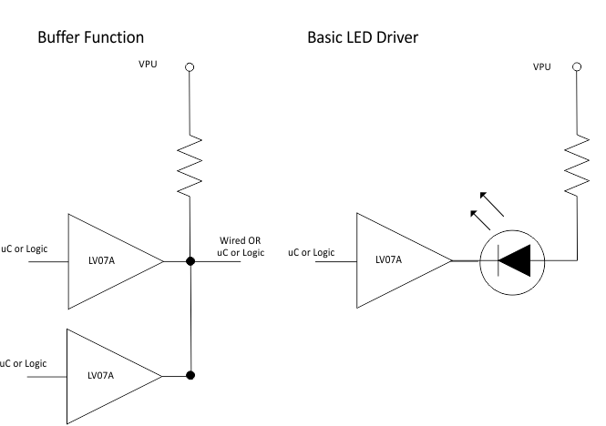 Figure 5. Typical Application Schematic
10.2.1 Design Requirements
This device uses CMOS technology and is open drain, so it has low output drive only. Care should be taken to avoid bus contention, because it can drive currents that would exceed maximum limits. Parallel output drive can create fast edges into light loads, so routing and load conditions should be considered to prevent ringing.
10.2.2 Detailed Design Procedure
- Recommended Input Conditions:
- For rise time and fall time specifications, see Δt/ΔV in the Recommended Operating Conditions table.
- For specified high and low levels, see VIH and VIL in theRecommended Operating Conditions table.
- Inputs are overvoltage tolerant allowing them to go as high as 5.5 V at any valid VCC.
- Recommended Output Conditions:
- Load currents should not exceed 35 mA per output and 50 mA total for the part.
10.2.3 Application Curves
 Figure 6. Output During Power Up with 4 k Pullup at 3.3 V