SCLS384K September 1997 – May 2024 SN74LV240A
PRODMIX
- 1
- 1 Features
- 2 Applications
- 3 Description
- 4 Pin Configuration and Functions
-
5 Specifications
- 5.1 Absolute Maximum Ratings
- 5.2 ESD Ratings
- 5.3 Recommended Operating Conditions
- 5.4 Thermal Information
- 5.5 Electrical Characteristics
- 5.6 Switching Characteristics, VCC = 2.5 V ±0.2 V
- 5.7 Switching Characteristics, VCC = 3.3 V ±0.3 V
- 5.8 Switching Characteristics, VCC = 5 V ±0.5 V
- 5.9 Noise Characteristics
- 5.10 Operating Characteristics
- 5.11 Typical Characteristics
- 6 Parameter Measurement Information
- 7 Detailed Description
- 8 Application and Implementation
- 9 Device and Documentation Support
- 10Revision History
- 11Mechanical, Packaging, and Orderable Information
Package Options
Refer to the PDF data sheet for device specific package drawings
Mechanical Data (Package|Pins)
- DGV|20
- DB|20
- NS|20
- DW|20
- PW|20
Thermal pad, mechanical data (Package|Pins)
Orderable Information
3 Description
These octal buffers/drivers with inverted outputs are designed for 2V to 5.5V VCC operation.
The ’LV240A devices are designed specifically to improve both the performance and density of 3-state memory address drivers, clock drivers, and bus-oriented receivers and transmitters.
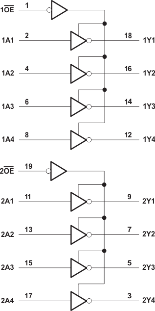
These devices are organized as two 4-bit buffers/line drivers with separate output-enable ( OE) inputs. When OE is low, the device passes inverted data from the A inputs to the Y outputs. When OE is high, the outputs are in the high-impedance state.
| PART NUMBER | PACKAGE(1) | PACKAGE SIZE(2) | BODY SIZE(3) |
|---|---|---|---|
| SN74LV240A | DGV (TVSOP, 20) | 5 mm × 6.4 mm | 5mm × 4.4mm |
| DB (SSOP, 20) | 7.2mm x 7.8mm | 7.2mm x 5.30mm | |
| DW (SOIC, 20) | 12.80mm x 10.3mm | 12.80mm x 7.50mm | |
| NS (SOP, 20) | 12.6mm x 7.8mm | 12.6mm x 5.3mm | |
| PW (TSSOP, 20) | 6.50mm x 6.4mm | 6.50mm x 4.40mm |
 Logic Diagram (Positive Logic)