SCLS392G April 1998 – February 2015 SN74LV86A
PRODUCTION DATA.
- 1 Features
- 2 Applications
- 3 Description
- 4 Simplified Schematic
- 5 Revision History
- 6 Pin Configuration and Functions
-
7 Specifications
- 7.1 Absolute Maximum Ratings
- 7.2 ESD Ratings
- 7.3 Recommended Operating Conditions
- 7.4 Thermal Information
- 7.5 Electrical Characteristics
- 7.6 Switching Characteristics, VCC = 2.5 V ±0.2 V
- 7.7 Switching Characteristics, VCC = 3.3 V ±0.3 V
- 7.8 Switching Characteristics, VCC = 5 V ±0.5 V
- 7.9 Noise Characteristics for SN74LV86A
- 7.10 Operating Characteristics
- 7.11 Typical Characteristics
- 8 Parameter Measurement Information
- 9 Detailed Description
- 10Application and Implementation
- 11Power Supply Recommendations
- 12Layout
- 13Device and Documentation Support
- 14Mechanical, Packaging, and Orderable Information
Package Options
Refer to the PDF data sheet for device specific package drawings
Mechanical Data (Package|Pins)
- D|14
- DB|14
- DGV|14
- PW|14
- NS|14
Thermal pad, mechanical data (Package|Pins)
Orderable Information
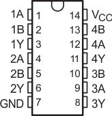
6 Pin Configuration and Functions
SN54LV86A: J or W Package
SN74LV86A: D, DB, DGV, NS, or PW Package
(Top View)
SN54LV86A: FK Package
(Top View)
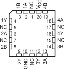
A. NC − No internal connection
Pin Functions
| PIN | I/O | DESCRIPTION |
|---|---|---|
| 1 | 1A | A input 1 |
| 2 | 1B | B input 1 |
| 3 | 1Y | Output 1 |
| 4 | 2A | A input 2 |
| 5 | 2B | B input 2 |
| 6 | 2Y | Output 2 |
| 7 | GND | ground |
| 8 | 3Y | Output 3 |
| 9 | 3A | A input 3 |
| 10 | 3B | B input 3 |
| 11 | 4Y | Output 4 |
| 12 | 4A | A input 4 |
| 13 | 4B | B input 4 |
| 14 | VCC | Power pin |