SCES635B JULY 2005 – April 2015 SN74LVCH16T245
PRODUCTION DATA.
- 1 Features
- 2 Applications
- 3 Description
- 4 Revision History
- 5 Description (continued)
- 6 Pin Configuration and Functions
-
7 Specifications
- 7.1 Absolute Maximum Ratings
- 7.2 ESD Ratings
- 7.3 Recommended Operating Conditions
- 7.4 Thermal Information
- 7.5 Electrical Characteristics
- 7.6 Switching Characteristics for VCCA = 1.8 V ±0.15 V
- 7.7 Switching Characteristics for VCCA = 2.5 V ±0.2 V
- 7.8 Switching Characteristics for VCCA = 3.3 V ±0.3 V
- 7.9 Switching Characteristics for VCCA = 5 V ±0.5 V
- 7.10 Operating Characteristics
- 7.11 Typical Characteristics
- 8 Parameter Measurement Information
- 9 Detailed Description
- 10Application and Implementation
- 11Power Supply Recommendations
- 12Layout
- 13Device and Documentation Support
- 14Mechanical, Packaging, and Orderable Information
Package Options
Mechanical Data (Package|Pins)
Thermal pad, mechanical data (Package|Pins)
Orderable Information
9 Detailed Description
9.1 Overview
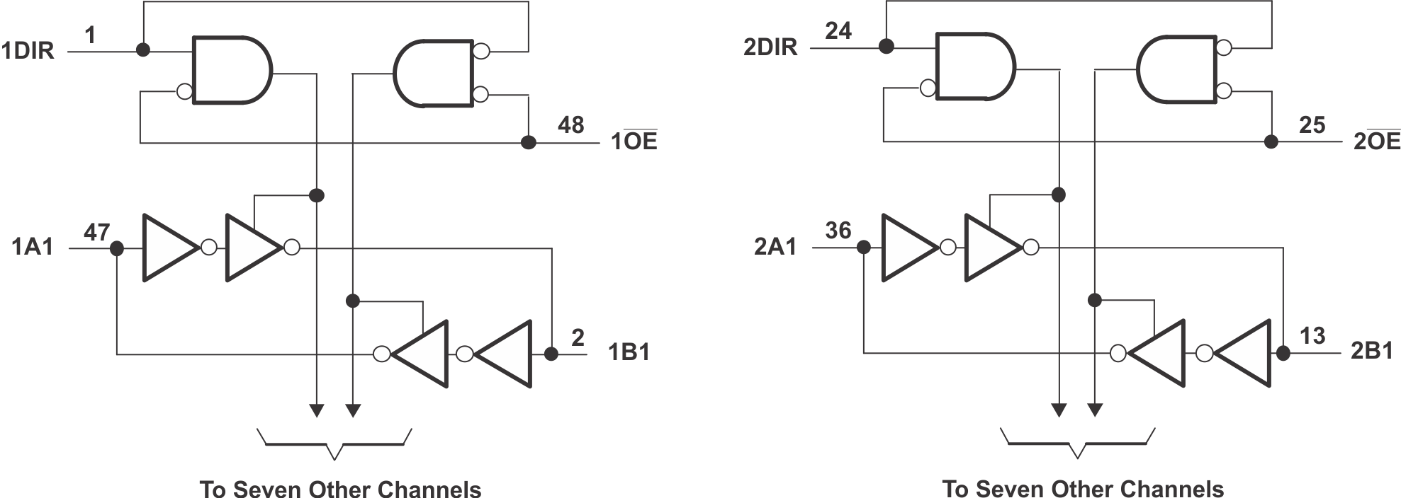
The SN74LVCH16T245 is a 16-bit, dual-supply noninverting bidirectional voltage level translation. Pins AX and control pins (DIR and OE) are supported by VCCA and pins BX are supported by VCCB. The A port is able to accept I/O voltages ranging from 1.65 V to 5.5 V, while the B port can accept I/O voltages from 1.65 V to 5.5 V. A high on DIR allows data transmission from A to B and a low on DIR allows data transmission from B to A when OE is set to low. When OE is set to high, both A and B are in the high-impedance state.
This device has Active bus-hold circuitry that holds unused or undriven inputs at a valid logic state. This device is fully specified for partial-power-down applications using off output current (Ioff).
The VCC isolation feature ensures that if either VCC input is at GND, both ports are put in a high-impedance state.
9.2 Functional Block Diagram

9.3 Feature Description
9.3.1 Fully Configurable Dual-Rail Design Allows Each Port to Operate Over the Full 1.65-V to 5.5-V Power-Supply Range
Both VCCA and VCCB can be supplied at any voltage from 1.65 V to 5.5 V making the device suitable for translating between any of the low voltage nodes (1.8-V, 2.5-V, and 3.3-V).
9.3.2 Support High-Speed Translation
SN74LVCH16T245 can support high data rate application. Data rates can be calculated form the maximum propagation delay. This is also dependant on the output load. For example, for a 3.3-V to 5-V conversion, the maximum frequency is 200 MHz.
9.3.3 Partial-Power-Down Mode Operation
This device is fully specified for partial-power-down applications using off output current (Ioff). Ioff will prevent backflow current by disabling I/O output circuits when device is in partial power-down mode.
9.3.4 VCC Isolation
The VCC isolation feature ensures that if either VCCA or VCCB are at GND, both ports will be in a high-impedance state (IOZ shown in Electrical Characteristics). This prevents false logic levels from being presented to either bus.
9.3.5 Bus Hold on Data Inputs
Active bus-hold circuitry holds unused or undriven inputs at a valid logic state. Use of pullup or pulldown resistors with the bus-hold circuitry is not recommended.
9.4 Device Functional Modes
The SN74LVCH16T245 is a voltage level translator that can operate from 1.65 V to 5.5 V (VCCA) and 1.65 V to 5.5 V (VCCB). The signal translation between 1.65 V and 5.5 V requires direction control and output enable control. When OE is low and DIR is high, data transmission is from A to B. When OE is low and DIR is low, data transmission is from B to A. When OE is high, both output ports will be high-impedance.
Table 1. Function Table (Each Transceiver)(1)
| CONTROL INPUTS | OUTPUT CIRCUITS | OPERATION | |||
|---|---|---|---|---|---|
| OE | DIR | A PORT | B PORT | ||
| L | L | Enabled | Hi-Z | B data to A bus | |
| L | H | Hi-Z | Enabled | A data to B bus | |
| H | X | Hi-Z | Hi-Z | Isolation | |