SLRS007C November 1986 – January 2015 SN754410
PRODUCTION DATA.
- 1 Features
- 2 Applications
- 3 Description
- 4 Simplified Schematic
- 5 Revision History
- 6 Pin Configuration and Functions
- 7 Specifications
- 8 Parameter Measurement Information
- 9 Detailed Description
- 10Application and Implementation
- 11Power Supply Recommendations
- 12Layout
- 13Device and Documentation Support
- 14Mechanical, Packaging, and Orderable Information
Package Options
Refer to the PDF data sheet for device specific package drawings
Mechanical Data (Package|Pins)
- NE|16
Thermal pad, mechanical data (Package|Pins)
Orderable Information
10 Application and Implementation
NOTE
Information in the following applications sections is not part of the TI component specification, and TI does not warrant its accuracy or completeness. TI’s customers are responsible for determining suitability of components for their purposes. Customers should validate and test their design implementation to confirm system functionality.
10.1 Application Information
Provide a 5-V supply to VCC1 and valid logic input levels to data and enable inputs. VCC2 must be connected to a power supply capable of suppling the needed current and voltage demand for the loads connected to the outputs.
10.2 Typical Application
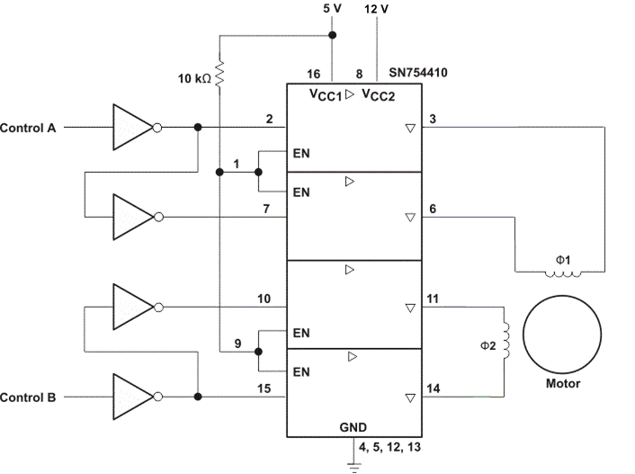 Figure 7. Typical Application Schematic
10.2.1 Design Requirements
The design techniques in the following sections may be used for applications which fall within the following requirements.
- 4.5-V minimum and 36-V maximum VCC2 voltage
- 1000-mA or less output current per channel
- 5-V supply with 10% tolerance or less
- TTL compatible logic inputs
10.2.2 Application Curves
Driver output voltage waveform with a two phase stepper motor; 12-V 20-Ω coils.
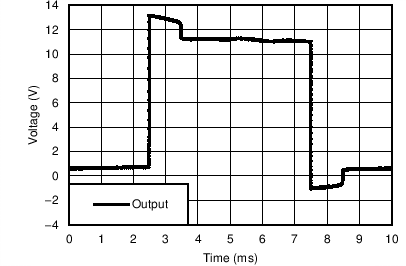 100 Hz Driver Output Waveform