SLRS021D December 1967 – January 2017 SN55451B , SN55452B , SN55453B , SN55454B , SN75451B , SN75452B , SN75453B , SN75454B
PRODUCTION DATA.
- 1 Features
- 2 Applications
- 3 Description
- 4 Revision History
- 5 Device Comparison Table
- 6 Pin Configuration and Functions
- 7 Specifications
- 8 Parameter Measurement Information
- 9 Detailed Description
- 10Application and Implementation
- 11Power Supply Recommendations
- 12Layout
- 13Device and Documentation Support
- 14Mechanical, Packaging, and Orderable Information
Package Options
Refer to the PDF data sheet for device specific package drawings
Mechanical Data (Package|Pins)
- D|8
- P|8
- PS|8
Thermal pad, mechanical data (Package|Pins)
- PS|8
Orderable Information
12 Layout
12.1 Layout Guidelines
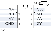
Thin traces can be used on the input due to the low-current logic that is used to drive the SNx545xB devices. Take care to separate the input channels to eliminate crosstalk. These traces are recommended for the output to be able to drive high currents. Be sure to connect ground or VCC to any unused input channels, and use a bypass capacitor on the VCC pin to prevent any power glitches.
12.2 Layout Example
 Figure 21. SN75451BD Layout