SLLS540C July 2002 – June 2021 SN65C3232 , SN75C3232
PRODUCTION DATA
- 1 Features
- 2 Applications
- 3 Description
- 4 Revision History
- 5 Pin Configuration and Functions
-
6 Specifications
- 6.1 Absolute Maximum Ratings
- 6.2 ESD Ratings
- 6.3 Recommended Operating Conditions
- 6.4 Thermal Information
- 6.5 Electrical Characteristics
- 6.6 Driver Section - Electrical Characteristics
- 6.7 Switching Characteristics
- 6.8 Receiver Section - Electrical Characteristics
- 6.9 Switching Characteristics
- 6.10 Typical Characteristics
- 7 Parameter Measurement Information
- 8 Detailed Description
- 9 Application and Implementation
- 10Layout
- 11Device and Documentation Support
- 12Mechanical, Packaging, and Orderable Information
Package Options
Refer to the PDF data sheet for device specific package drawings
Mechanical Data (Package|Pins)
- DB|16
- DW|16
- D|16
Thermal pad, mechanical data (Package|Pins)
- DW|16
Orderable Information
3 Description
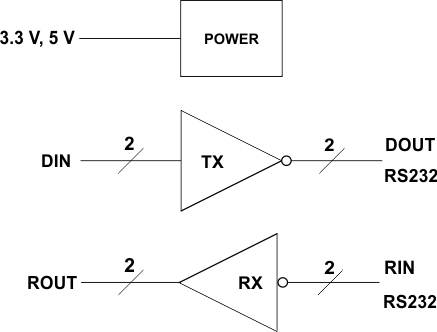
The SN65C3232 and SN75C3232 consist of two line drivers, two line receivers, and a dual charge-pump circuit with ±15-kV ESD protection pin-to-pin (serial-port connection pins, including GND). These devices provide the electrical interface between an asynchronous communication controller and the serial-port connector. The charge pump and four small external capacitors allow operation from a single 3-V to 5.5-V supply. The devices operate at typical data signaling rates up to 1 Mbit/s and a driver output slew rate of 24 V/μs to 150 V/μs.
| PART NUMBER | PACKAGE(1) | BODY SIZE (NOM) |
|---|---|---|
| SN65C3232 SN75C3232 |
D (SOIC) (16) | 9.90 mm x 3.91 mm |
| DB (SSOP) (16) | 6.20 mm x 5.30 mm | |
| DW (SOIC) (16) | 10.3 mm x 7.50 mm | |
| PW (TSSOP) (16) | 5.00 mm v 4.40 mm |
 Simplified Diagram