SLLS500B May 2001 – October 2023 SN65LBC182 , SN75LBC182
PRODUCTION DATA
- 1
- 1 Features
- 2 Applications
- 3 Description
- 4 Pin Configuration and Functions
-
5 Specifications
- 5.1 Absolute Maximum Ratings
- 5.2 ESD Ratings
- 5.3 Dissipation Rating
- 5.4 Recommended Operating Conditions
- 5.5 Thermal Information
- 5.6 Driver Electrical Characteristics
- 5.7 Receiver Electrical Characteristics
- 5.8 Driver Switching Characteristics
- 5.9 Receiver Switching Characteristics
- 5.10 Typical Characteristics
- 6 Parameter Measurement Information
- 7 Detailed Description
- 8 Application and Implementation
- 9 Device and Documentation Support
- 10Revision History
- 11Mechanical, Packaging, and Orderable Information
Package Options
Mechanical Data (Package|Pins)
Thermal pad, mechanical data (Package|Pins)
Orderable Information
3 Description
The SN65LBC182 and SN75LBC182 are differential data line transceivers with a high level of ESD protection in the trade-standard footprint of the SN75176. They are designed for balanced transmission lines and meet ANSI standard TIA/EIA-485-A and ISO 8482. The SN65LBC182 and SN75LBC182 combine a 3-state, differential line driver and differential input line receiver, both of which operate from a single 5-V power supply. The driver and receiver have active-high and active-low enables, respectively, which can be externally connected together to function as a direction control.
The driver outputs and the receiver inputs connect internally to form a differential input/output (I/O) bus port that is designed to offer minimum loading to the bus. This port operates over a wide range of common-mode voltage, making the device suitable for party-line applications. The device also includes additional features for party-line data buses in electrically noisy environment applications such as industrial process control or power inverters.
The SN75LBC182 and SN65LBC182 bus pins also exhibit a high input resistance equivalent to one-fourth unit load allowing connection of up to 128 similar devices on the bus. The high ESD tolerance protects the device for cabled connections. (For an even higher level of protection, see the SN65/75LBC184, literature number SLLS236.)
The differential driver design incorporates slew-rate-controlled outputs sufficient to transmit data up to 250 kbps. Slew-rate control allows longer unterminated cable runs and longer stub lengths from the main backbone than possible with uncontrolled voltage transitions. The receiver design provides a fail-safe output of a high level when the inputs are left floating (open circuit). Very low device supply current can be achieved by disabling the driver and the receiver.
The SN65LBC182 is characterized for operation from −40°C to 85°C, and the SN75LBC182 is characterized for operation from 0°C to 70°C.
| PART NUMBER | PACKAGE(1) | PACKAGE SIZE(2) |
|---|---|---|
| SN65LBC182, SN75LBC182 |
P (PDIP, 8) | 9.81 mm × 9.43 mm |
| D (SOIC, 8) | 4.9 mm × 6 mm |
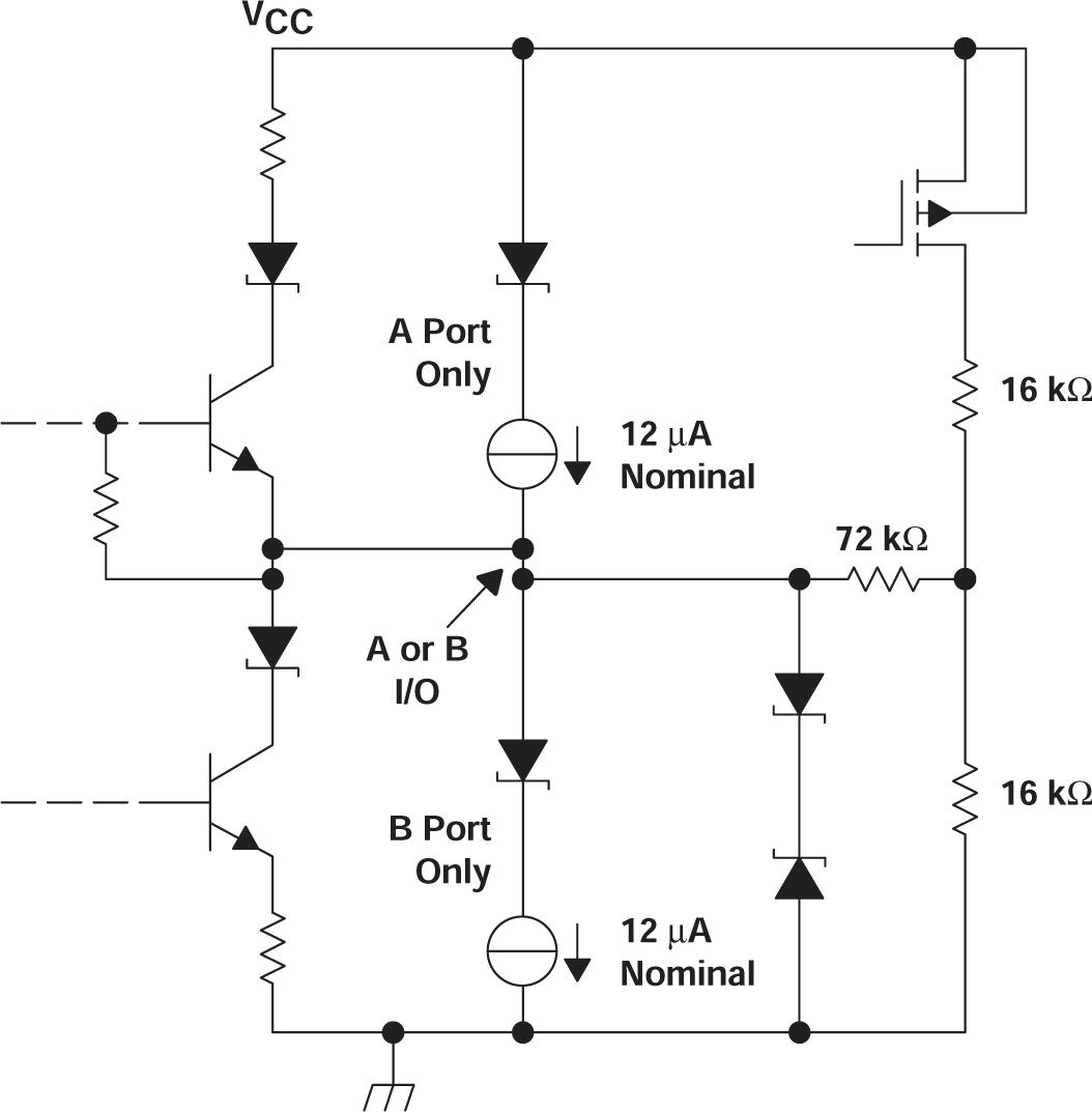
 Schematic of Inputs and Outputs