SLLSE63A December 2010 – May 2016 SN75LVCP600
PRODUCTION DATA.
- 1 Features
- 2 Applications
- 3 Description
- 4 Revision History
- 5 Description (continued)
- 6 Pin Configuration and Functions
- 7 Specifications
- 8 Parameter Measurement Information
- 9 Detailed Description
- 10Application and Implementation
- 11Power Supply Recommendations
- 12Layout
- 13Device and Documentation Support
- 14Mechanical, Packaging, and Orderable Information
Package Options
Mechanical Data (Package|Pins)
- DRF|8
Thermal pad, mechanical data (Package|Pins)
- DRF|8
Orderable Information
10 Application and Implementation
NOTE
Information in the following applications sections is not part of the TI component specification, and TI does not warrant its accuracy or completeness. TI’s customers are responsible for determining suitability of components for their purposes. Customers should validate and test their design implementation to confirm system functionality.
10.1 Application Information
The SN75LVCP600 is a single-channel SATA redriver and signal conditioner supporting data rates up to 6 Gbps. The inputs incorporate an out-of-band (OOB) detector, which automatically squelches the output while maintaining a stable common-mode voltage compliant to the SATA link.
10.2 Typical Application
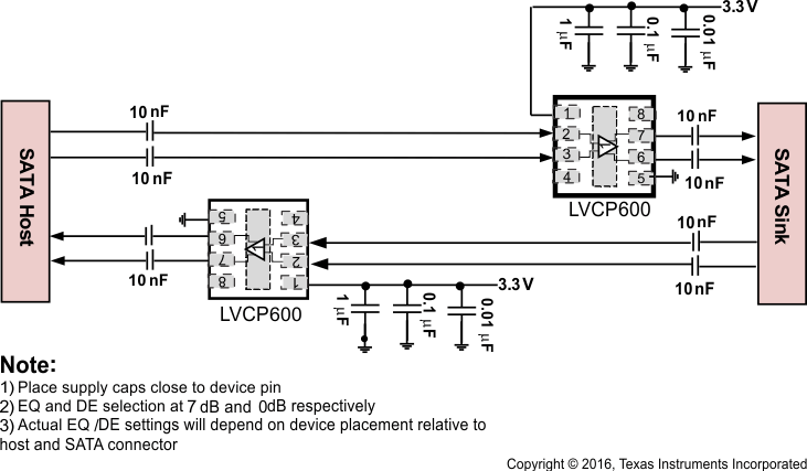 Figure 10. Typical Device Implementation
10.2.1 Design Requirements
This design requires layout flexibility to place 0-Ω resistors. If a redriver is needed, go to step 3 in Detailed Design Procedure.
Table 2. Design Parameters
| DESIGN PARAMETER | VALUE |
|---|---|
| VCC | 3.3 V |
| ICC | 29 mA |
| Input voltage | 120 mVpp to 1.6 Vpp |
| Output voltage | 400 mVpp to 900 mVpp |
10.2.2 Detailed Design Procedure
The LVCP600 allows the user to take the guess work of using a signal conditioning device in a SATA link. With the SN75LVCP600, the user has the option to use or remove the device based on signal conditioning needs. See Figure 11.
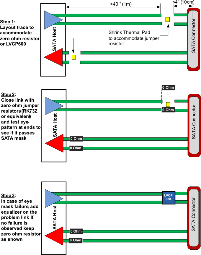 Figure 11. Implementation Guideline
Figure 13 through Figure 22 show SN75LVCP600 typical performance plots when connected to various trace lengths with VCC = 3.3 V and TA = 25°C. All eye diagrams measured using K28.5 pattern at 6 Gbps. Figure 12 shows the setup for the performance plots in Application Curves.
 Figure 12. Test Points
10.2.3 Application Curves
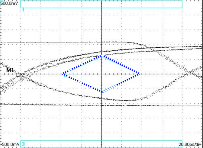
| DE = 1 | EQ = 0 |
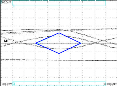
| DE = 1 | EQ = 0 |
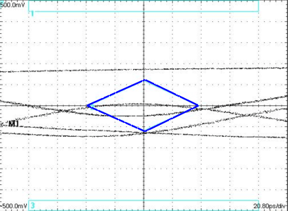
| DE = 1 | EQ = 0 |
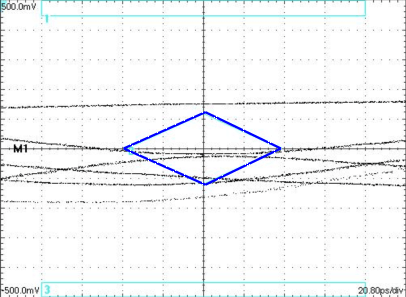
| DE = 1 | EQ = 1 |
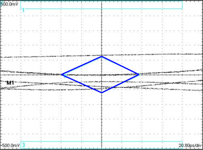
| DE = 1 | EQ = 1 |
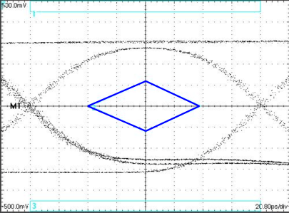
| DE = 1 | EQ = 0 |
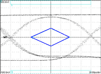
| DE = 1 | EQ = 0 |
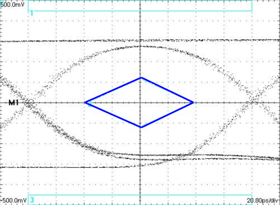
| DE = 1 | EQ = 0 |
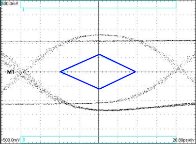
| DE = 1 | EQ = 1 |
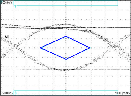
| DE = 1 | EQ = 1 |