SLLSE41H June 2010 – March 2016 SN75LVCP601
PRODUCTION DATA.
- 1 Features
- 2 Applications
- 3 Description
- 4 Revision History
- 5 Pin Configuration and Functions
- 6 Specifications
- 7 Parameter Measurement Information
- 8 Detailed Description
- 9 Application and Implementation
- 10Power Supply Recommendations
- 11Layout
- 12Device and Documentation Support
- 13Mechanical, Packaging, and Orderable Information
Package Options
Mechanical Data (Package|Pins)
- RTJ|20
Thermal pad, mechanical data (Package|Pins)
- RTJ|20
Orderable Information
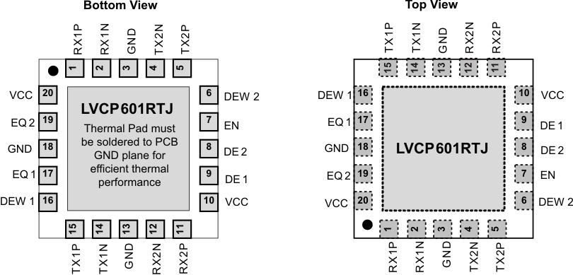
5 Pin Configuration and Functions
RTJ Package
16-Pin WQFN With Thermal Pad

Pin Functions
| PIN | PIN TYPE | DESCRIPTION | |
|---|---|---|---|
| NAME | NO. | ||
| CONTROL PINS | |||
| DE1(1) | 9 | I, LVCMOS | Selects de-emphasis settings for CH 1 and CH 2 per Table 1. Internally tied to VCC / 2. |
| DE2(1) | 8 | ||
| DEW1 | 16 | I, LVCMOS | De-emphasis width control for CH 1 and CH 2. 0 = De-emphasis pulse duration, short 1 = De-emphasis pulse duration, long (default) |
| DEW2 | 6 | ||
| EN | 7 | I, LVCMOS | Device enable and disable pin, internally pulled to VCC. 0 = Device in standby mode 1 = Device enabled (default) |
| EQ1(1) | 17 | I, LVCMOS | Selects equalization settings for CH 1 and CH 2 per Table 1. Internally tied to VCC / 2. |
| EQ2(1) | 19 | ||
| HIGH-SPEED DIFFERENTIAL I/O | |||
| RX1N | 2 | I, CML | Noninverting and inverting CML differential input for CH 1 and CH 2. These pins connect to an internal voltage bias via a dual-termination resistor circuit. |
| RX1P | 1 | I, CML | |
| RX2N | 12 | I, CML | |
| RX2P | 11 | I, CML | |
| TX1N | 14 | O, VML | Noninverting and inverting VML differential output for CH 1 and CH 2. These pins connect internally to voltage bias via termination resistors. |
| TX1P | 15 | O, VML | |
| TX2N | 4 | O, VML | |
| TX2P | 5 | O, VML | |
| POWER | |||
| GND | 3, 13, 18 | Power | Supply ground |
| VCC | 10, 20 | Power | Positive supply must be 3.3 V ± 10% |
(1) Internally biased to VCC / 2 with >200-kΩ pullup or pulldown. When 3-state pins are left as NC, board leakage at the pin pad must be <1 µA; otherwise, drive to VCC / 2 to assert mid-level state.