SLAS978B September 2013 – February 2014 TAS2553
PRODUCTION DATA.
- 1 Features
- 2 Applications
- 3 Description
- 4 Revision History
- 5 Terminal Configuration and Functions
- 6 Specifications
-
7 Detailed Description
- 7.1 Overview
- 7.2 Functional Block Diagram
- 7.3 Feature Description
- 7.4 Device Functional Modes
- 7.5
Register Map
- 7.5.1 Register Map Summary
- 7.5.2 Register 0x00: Device Status Register
- 7.5.3 Register 0x01: Configuration Register 1
- 7.5.4 Register 0x02: Configuration Register 2
- 7.5.5 Register 0x03: Configuration Register 3
- 7.5.6 Register 0x04: DOUT Tristate Mode
- 7.5.7 Register 0x05: Serial Interface Control Register 1
- 7.5.8 Register 0x06: Serial Interface Control Register 2
- 7.5.9 Register 0x07: Output Data Register
- 7.5.10 Register 0x08: PLL Control Register 1
- 7.5.11 Register 0x09: PLL Control Register 2
- 7.5.12 Register 0x0A: PLL Control Register 3
- 7.5.13 Register 0x0B: Battery Tracking Inflection Point Register
- 7.5.14 Register 0x0C: Battery Tracking Slope Control Register
- 7.5.15 Register 0x0D: Reserved Register
- 7.5.16 Register 0x0E: Battery Tracking Limiter Attack Rate and Hysteresis Time
- 7.5.17 Register 0x0F: Battery Tracking Limiter Release Rate
- 7.5.18 Register 0x10: Battery Tracking Limiter Integration Count Control
- 7.5.19 Register 0x11: PDM Configuration Register
- 7.5.20 Register 0x12: PGA Gain Register
- 7.5.21 Register 0x13: Class-D Edge Rate Control Register
- 7.5.22 Register 0x14: Boost Auto-Pass Through Control Register
- 7.5.23 Register 0x15: Reserved Register
- 7.5.24 Register 0x16: Version Number
- 7.5.25 Register 0x17: Reserved Register
- 7.5.26 Register 0x18: Reserved Register
- 7.5.27 Register 0x19: VBAT Data Register
- 8 Applications and Implementation
- 9 Power Supply Recommendations
- 10Layout
- 11Device and Documentation Support
- 12Mechanical, Packaging, and Orderable Information
Package Options
Mechanical Data (Package|Pins)
- YFF|30
Thermal pad, mechanical data (Package|Pins)
Orderable Information
10 Layout
10.1 Layout Guidelines
- Place the boost inductor between VBAT and SW close to device terminals with no VIAS between the device terminals and the inductor.
- Place the capacitor between VREG and VBOOST close to device terminals with no VIAS between the device terminals and capacitor.
- Place the capacitor between VBOOST/PVDD and GND close to device terminals with no VIAS between the device terminals and capacitor.
- Do not use VIAS for traces that carry high current. These include the traces for VBOOST, SW, PVDD and the speaker OUT+, OUT-.
- Use epoxy filled vias for the interior pads.
- Connect VSENSE+, VSENSE- as close as possible to the speaker.
- VSENSE+, VSENSE- should be connected between the EMI ferrite and the speaker if EMI ferrites are used on OUT+, OUT-.
- VSENSE+, VSENSE- should be connected between the EMI ferrite and the EMI capacitor if EMI capacitors are used. EMI ferrites must be used if EMI capacitors are used on OUT+, OUT-.
- If the analog inputs, IN+ and IN-, are:
- used, analog input traces should be routed symmetrically for true differential performance.
- used, do not run analog input traces parallel to digital lines.
- used, they should be ac coupled.
- not used, they should be shorted together.
- Use a ground plane with multiple vias for each terminal to create a low-impedance connection to GND for minimum ground noise.
- Use supply decoupling capacitors as shown in Figure 51 and Figure 56 and described in Power Supply Recommendations.
- Place EMI ferrites, if used, close to the device.
10.2 Layout Example
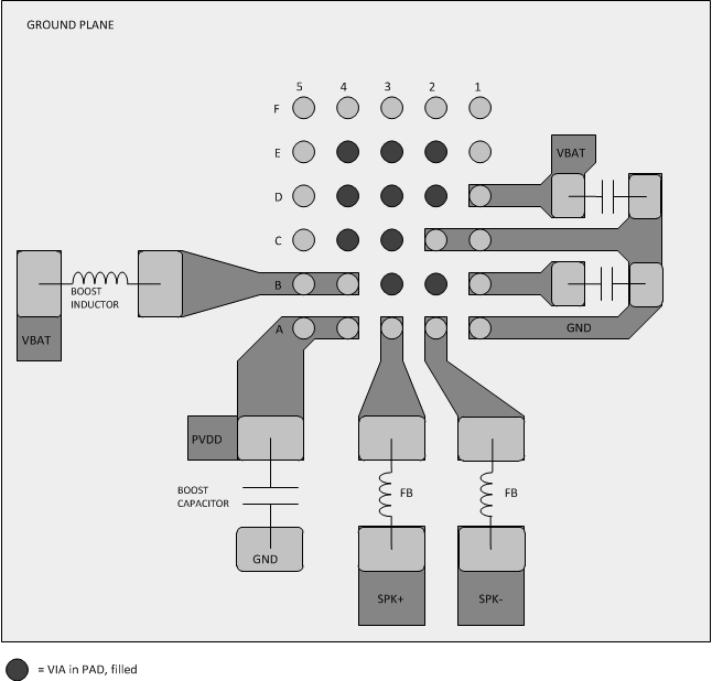 Figure 60. TAS2553 Board Layout
10.3 Package Dimensions
The TAS2553 uses a 30-ball, 0.4 mm pitch WCSP package. The die length (D) and width (E) correspond to the package mechanical drawing at the end of the datasheet.
| DIMENSION | D | E |
|---|---|---|
| Max | 2885 μm | 2605 μm |
| Typ | 2855 μm | 2575 μm |
| Min | 2825 μm | 2545 μm |