SLAS988B June 2014 – August 2015 TAS5756M
PRODUCTION DATA.
- 1 Features
- 2 Applications
- 3 Description
- 4 Revision History
- 5 Device Comparison Table
- 6 Pin Configuration and Functions
-
7 Specifications
- 7.1 Absolute Maximum Ratings
- 7.2 ESD Ratings
- 7.3 Recommended Operating Conditions
- 7.4 Thermal Information
- 7.5 Electrical Characteristics
- 7.6 MCLK Timing
- 7.7 Serial Audio Port Timing - Slave Mode
- 7.8 Serial Audio Port Timing - Master Mode
- 7.9 I2C Bus Timing - Standard
- 7.10 I2C Bus Timing - Fast
- 7.11 SPK_MUTE Timing
- 7.12 Power Dissipation
- 7.13 Typical Characteristics
-
8 Detailed Description
- 8.1 Overview
- 8.2 Functional Block Diagram
- 8.3
Feature Description
- 8.3.1 Power-on-Reset (POR) Function
- 8.3.2 Device Clocking
- 8.3.3
Serial Audio Port
- 8.3.3.1 Clock Master Mode from Audio Rate Master Clock
- 8.3.3.2 Clock Master from a Non-Audio Rate Master Clock
- 8.3.3.3 Clock Slave Mode with 4-Wire Operation (SCLK, MCLK, LRCK/FS, SDIN)
- 8.3.3.4 Clock Slave Mode with SLCK PLL to Generate Internal Clocks (3-Wire PCM)
- 8.3.3.5 Serial Audio Port - Data Formats and Bit Depths
- 8.3.3.6 Input Signal Sensing (Power-Save Mode)
- 8.3.3.7 Serial Data Output
- 8.3.4 Modulation Scheme
- 8.3.5 miniDSP Audio Processing Engine
- 8.3.6 Adjustable Amplifier Gain and Switching Frequency Selection
- 8.3.7
Error Handling and Protection Suite
- 8.3.7.1 Device Overtemperature Protection
- 8.3.7.2 SPK_OUTxx Overcurrent Protection
- 8.3.7.3 DC Offset Protection
- 8.3.7.4 Internal VAVDD Undervoltage-Error Protection
- 8.3.7.5 Internal VPVDD Undervoltage-Error Protection
- 8.3.7.6 Internal VPVDD Overvoltage-Error Protection
- 8.3.7.7 External Undervoltage-Error Protection
- 8.3.7.8 Internal Clock Error Notification (CLKE)
- 8.3.8 GPIO Port and Hardware Control Pins
- 8.3.9 I2C Communication Port
- 8.4 Device Functional Modes
-
9 Application and Implementation
- 9.1 Application Information
- 9.2
Typical Applications
- 9.2.1 2.0 (Stereo BTL) System
- 9.2.2 Mono (PBTL) Systems
- 9.2.3 2.1 (Stereo BTL + External Mono Amplifier) Systems
- 9.2.4 2.2 (Dual Stereo BTL) Systems
- 9.2.5 1.1 (Dual BTL, Bi-Amped) Systems
- 10Power Supply Recommendations
- 11Layout
- 12Device and Documentation Support
- 13Mechanical, Packaging, and Orderable Information
Package Options
Mechanical Data (Package|Pins)
- DCA|48
Thermal pad, mechanical data (Package|Pins)
- DCA|48
Orderable Information
8 Detailed Description
8.1 Overview
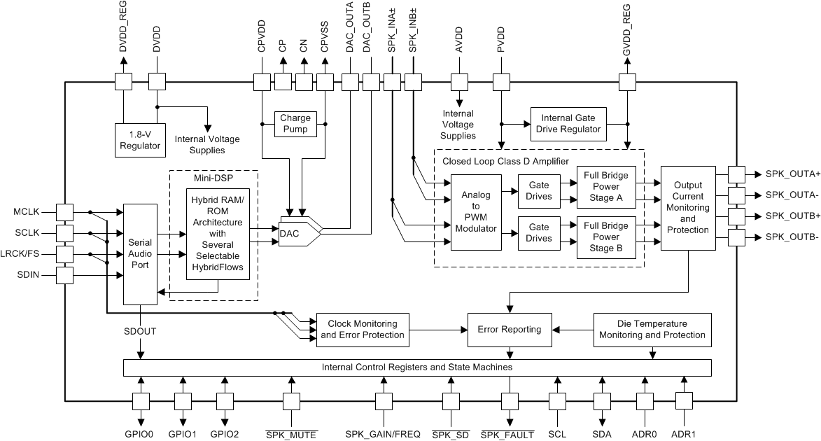
The TAS5756M device integrates 4 main building blocks together into a single cohesive device that maximizes sound quality, flexibility, and ease of use. The 4 main building blocks are listed as follows:
- A stereo audio DAC, boasting a strong Burr-Brown heritage with a highly flexible serial audio port.
- A miniDSP audio processing core with HybridFlow architecture, which provides an increase in flexibility over a fixed-function ROM device with faster download time than a fully programmable device
- A flexible closed-loop amplifier capable of operating in stereo or mono, at several different switching frequencies, and with a variety of output voltages and loads.
- An I2C control port for communication with the device
The device requires only two power supplies for proper operation. A DVDD supply is needed to power the low-voltage digital and analog circuitry. Another supply, called PVDD, is needed to provide power to the output stage of the audio amplifier. The operating range for these supplies is shown in theRecommended Operating Conditions table.
Communication with the device is accomplished through the I2C control port. A speaker amplifier fault line is also provided to notify a system controller of the occurrence of an overtemperature, overcurrent, overvoltage, undervoltage, or DC error in the speaker amplifier. There are three digital GPIO pins that are available for use by the HybridFlows. One popular use of the GPIO lines is to provide a Serial Audio Output from the device (SDOUT). HybridFlows which provide an SDOUT customarily present that signal on GPIO2, although this configuration can be changed via the I2C control port. The register space in the control port spans several pages to accommodate some static controls which maintain their functionality across HybridFlows, as well as controls that are determined by the HybridFlow used.
The MiniDSP audio processing core, featuring a HybridFlow architecture, allows the selection of a configurable DSP program called a HybridFlow from a list of available HybridFlows. A hybrid flow combines audio processing blocks, many of which that are built in the ROM portion of the device, together in a single payload. The PurePath™ Console GUI provides a means by which to select the HybridFlow and manipulate the controls associated with that HybridFlow.
8.2 Functional Block Diagram
8.3 Feature Description
8.3.1 Power-on-Reset (POR) Function
The TAS5756M device has a power-on reset function. This feature resets all of the registers to their default configuration as the device is powering up. When the low-voltage power supply used to power DVDD, AVDD, and CPVDD exceeds the POR threshold, the device holds sets all of the internal registers to their default values and holds them there until it receives valid MCLK, SCLK, and LRCK/FS toggling for a period of approximately 4 ms. After the toggling period has passed, the internal reset of the registers is removed and the registers can be programmed via the I2C Control Port.
8.3.2 Device Clocking
The TAS5756M devices have flexible systems for clocking. Internally, the device requires a number of clocks, mostly at related clock rates to function correctly. All of these clocks can be derived from the Serial Audio Interface in one form or another.
 Figure 60. Audio Flow with Respective Clocks
Figure 60 shows the basic data flow at basic sample rate (fS). When the data is brought into the serial audio interface, it is processed, interpolated and modulated to 128 × fS before arriving at the current segments for the final digital to analog conversion.
Figure 61 shows the clock tree.
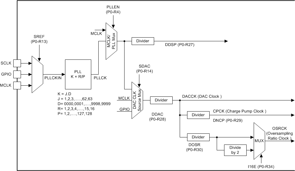 Figure 61. TAS5756M Clock Distribution Tree
The Serial Audio Interface typically has 4 connection pins which are listed as follows:
- MLCK (System Master Clock)
- SLCK (Bit Clock)
- LRCK/FS (Left Right Word Clock and Frame Sync)
- SDIN (Input Data. The output date, SDOUT, is presented on one of the GPIO pins. See theSerial Data Output section)
The device has an internal PLL that is used to take either MLCK or SLCK and create the higher rate clocks required by the and the DAC clock.
In situations where the highest audio performance is required, bringing MLCK to the device along with SLCK and LRCK/FS is recommended. The device should be configured so that the PLL is only providing a clock source to the DSP. All other clocks are then a division of the incoming MLCK. To enable the MCLK as the main source clock, with all others being created as divisions of the incoming MCLK, set the DAC CLK source Mux (SDAC in Figure 61) to use MLCK as a source, rather than the output of the MLCK/PLL Mux.
8.3.3 Serial Audio Port
8.3.3.1 Clock Master Mode from Audio Rate Master Clock
In Master Mode, the device generates bit clock and left-right and frame sync clock and outputs them on the appropriate pins. To configure the device in this mode, first put the device into reset, then use registers SLCKO and LRKO (P0-R9). Then reset the LRCK/FS and SCLK divider counters using bits RSLCK and RLRK (P0-R12). Finally, exit reset.
Figure 62 shows a simplified serial port clock tree for the device in master mode.
 Figure 62. Simplified Clock Tree for MLCK Sourced Master Mode
In master mode, MLCK is an input and SCLK and LRCK/FS are outputs. SCLK and LRCK/FS are integer divisions of MLCK. Master mode with a non-audio rate master clock source requires external GPIO’s to use the PLL in standalone mode. The PLL needs to be configured to ensure that the on-chip processor can be driven at its maximum clock rate. This mode of operation is described in theClock Master from a Non-Audio Rate Master Clock section.
When used with audio rate master clocks, the register changes that need to be done include switching the device into master mode, and setting the divider ratio. An example of this mode of operations is using 24.576 MCLK as a master clock source and driving the SCLK and LRCK/FS with integer dividers to create 48 kHz. In this mode, the DAC section of the device is also running from the PLL output. The TAS5756M device is able to meet the specified audio performance while using the internal PLL. However, using the MCLK CMOS oscillator source will have less jitter than the PLL.
To switch the DAC clocks (SDAC in the Figure 61) the following registers should be modified
- Clock Tree Flex Mode (P253-R63 and P253-R64)
- DAC and OSR Source Clock Register (P0-R14). Set to 0x30 (MLCK input, and OSR is set to whatever the DAC source is)
- The DAC clock divider should be 16fS.
- 16 × 48 kHz = 768 kHz
- 24.576 MHz (MLCK in) / 768 kHz = 32
- Therefore, the divide ratio for register DDAC (P0-R28) should be set to 32. The register mapping gives 0x00 = 1, so 32 must be converter to 0x1F (31dec).
8.3.3.2 Clock Master from a Non-Audio Rate Master Clock
The classic example here is running 12-MHz Master clock for a 48-kHz sampling system. Given the clock tree for the device (shown in Figure 61), a non-audio clock rate cannot be brought into the MLCK to the PLL in master mode. Therefore, the PLL source must be configured to be a GPIO pin, and the output brought back into another GPIO pin.
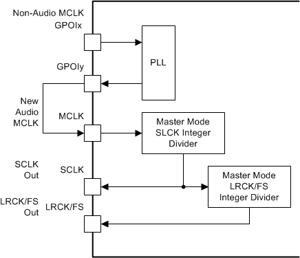 Figure 63. Generating Audio Clocks Using Non-Audio Clock Sources
The clock flow through the system is shown in Figure 63. The newly generated MLCK must be brought out of the device on a GPIO pin, then brought into the MLCK pin for integer division to create SCLK and LRCK/FS outputs.
NOTE
Pullup resistors should be used on SCLK and LRCK/FS in this mode to ensure the device remains out of sleep mode.
8.3.3.3 Clock Slave Mode with 4-Wire Operation (SCLK, MCLK, LRCK/FS, SDIN)
The TAS5756M device requires a system clock to operate the digital interpolation filters and advanced segment DAC modulators. The system clock is applied at the MLCK input and supports up to 50 MHz. The TAS5756M device system-clock detection circuit automatically senses the system-clock frequency. Common audio sampling frequencies in the bands of 8 kHz, 16 kHz, (32 kHz – 44.1 kHz – 48kHz), (88.2 kHz – 96 kHz), and (176.4 kHz – 192 kHz) are supported.
NOTE
Values in the parentheses are grouped when detected, for example, 88.2 kHz and 96 kHz are detected as double rate, 32 kHz, 44.1 kHz and 48 kHz are detected as single rate and so on.
In the presence of a valid bit MCLK, SCLK and LRCK/FS, the device automatically configures the clock tree and PLL to drive the miniDSP as required.
The sampling frequency detector sets the clock for the digital filter, Delta Sigma Modulator (DSM) and the Negative Charge Pump (NCP) automatically. Table 2 shows examples of system clock frequencies for common audio sampling rates.
MLCK rates that are not common to standard audio clocks, between 1 MHz and 50 MHz, are supported by configuring various PLL and clock-divider registers directly. In this mode, auto clock mode should be disabled using P0-R37. Additionally, it may be necessary to ignore clock error detection if external clocks are not-available for some time during configuration or if the clocks presented on the pins of the device or are invalid. This extended programmability allows the device to operate in an advanced mode in which it becomes a clock master and drive the host serial port with LRCK/FS and SLCK, from a non-audio related clock (for example, using a setting of 12 MHz to generate 44.1 kHz [LRCK/FS] and 2.8224 MHz [SLCK]).
Table 2 shows the timing requirements for the system clock input. For optimal performance, use a clock source with low phase jitter and noise. For MCLK timing requirements, refer to the Serial Audio Port Timing – Master Mode section.
Table 2. System Master Clock Inputs for Audio Related Clocks
| SAMPLING FREQUENCY |
SYSTEM CLOCK FREQUENCY (fMLCK) (MHz) | |||||
|---|---|---|---|---|---|---|
| 64 fS | 128 fS | 192 fS | 256 fS | 384 fS | 512 fS | |
| 8 kHz | See(1) | 1.024(2) | 1.536(2) | 2.048 | 3.072 | 4.096 |
| 16 kHz | 2.048(2) | 3.072(2) | 4.096 | 6.144 | 8.192 | |
| 32 kHz | 4.096(2) | 6.144(2) | 8.192 | 12.288 | 16.384 | |
| 44.1 kHz | 5.6488(2) | 8.4672(2) | 11.2896 | 16.9344 | 22.5792 | |
| 48 kHz | 6.144(2) | 9.216(2) | 12.288 | 18.432 | 24.576 | |
| 88.2 kHz | 11.2896(2) | 16.9344 | 22.5792 | 33.8688 | 45.1584 | |
| 96 kHz | 12.288(2) | 18.432 | 24.576 | 36.864 | 49.152 | |
| 176.4 kHz | 22.5792 | 33.8688 | 45.1584 | See(1) | See(1) | |
| 192 kHz | 24.576 | 36.864 | 49.152 | |||
8.3.3.4 Clock Slave Mode with SLCK PLL to Generate Internal Clocks (3-Wire PCM)
8.3.3.4.1 Clock Generation using the PLL
The TAS5756M device supports a wide range of options to generate the required clocks as shown in Figure 61.
The clocks for the PLL require a source reference clock. This clock is sourced as the incoming SLCK or MLCK, a GPIO can also be used.
The source reference clock for the PLL reference clock is selected by programming the SRCREF value on P0-R13, B[6:4]. The TAS5756M device provides several programmable clock dividers to achieve a variety of sampling rates. See Figure 61.
If PLL functionality is not required, set the PLLEN value on P0-R4, B[0] to 0. In this situation, an external master clock is required.
Table 3. PLL Configuration Registers
| CLOCK MULTIPLEXER | ||
|---|---|---|
| REGISTER | FUNCTION | BITS |
| SREF | PLL Reference | P0-R13, B[6:4] |
| DDSP | clock divider | P0-R27, B[6:0] |
| DSLCK | External SLCK Div | P0-R32, B[6:0] |
| DLRK | External LRCK/FS Div | P0-R33, B[7:0] |
8.3.3.4.2 PLL Calculation
The TAS5756M device has an on-chip PLL with fractional multiplication to generate the clock frequency needed by the Digital Signal Processing blocks. The programmability of the PLL allows operation from a wide variety of clocks that may be available in the system. The PLL input (PLLCKIN) supports clock frequencies from 1 MHz to 50 MHz and is register programmable to enable generation of required sampling rates with fine precision.
The PLL is enabled by default. The PLL can be enabled by writing to P0-R4, B[0]. When the PLL is enabled, the PLL output clock PLLCK is given by Equation 1:

where
- R = 1, 2, 3,4, ... , 15, 16
- J = 4,5,6, . . . 63, and D = 0000, 0001, 0002, . . . 9999
- K = [J value].[D value]
- P = 1, 2, 3, ... 15
R, J, D, and P are programmable. J is the integer portion of K (the numbers to the left of the decimal point), while D is the fractional portion of K (the numbers to the right of the decimal point, assuming four digits of precision).
8.3.3.4.2.1 Examples:
- If K = 8.5, then J = 8, D = 5000
- If K = 7.12, then J = 7, D = 1200
- If K = 14.03, then J = 14, D = 0300
- If K = 6.0004, then J = 6, D = 0004
When the PLL is enabled and D = 0000, the following conditions must be satisfied:
- 1 MHz ≤ ( PLLCKIN / P ) ≤ 20 MHz
- 64 MHz ≤ (PLLCKIN x K x R / P ) ≤ 100 MHz
- 1 ≤ J ≤ 63
When the PLL is enabled and D ≠ 0000, the following conditions must be satisfied:
- 6.667 MHz ≤ PLLCLKIN / P ≤ 20 MHz
- 64 MHz ≤ (PLLCKIN x K x R / P ) ≤ 100 MHz
- 4 ≤ J ≤ 11
- R = 1
When the PLL is enabled,
- fS = (PLLCLKIN × K × R) / (2048 × P)
- The value of N is selected so that fS × N = PLLCLKIN x K x R / P is in the allowable range.
Example: MCLK = 12 MHz and fS = 44.1 kHz, (N=2048)
Select P = 1, R = 1, K = 7.5264, which results in J = 7, D = 5264
Example: MCLK = 12 MHz and fS = 48.0 kHz, (N=2048)
Select P = 1, R = 1, K = 8.192, which results in J = 8, D = 1920
Values are written to the registers in Table 4.
Table 4. PLL Registers
| DIVIDER | FUNCTION | BITS |
|---|---|---|
| PLLE | PLL enable | P0-R4, B[0] |
| PPDV | PLL P | P0-R20, B[3:0] |
| PJDV | PLL J | P0-R21, B[5:0] |
| PDDV | PLL D | P0-R22, B[5:0] |
| P0-R23, B[7:0] | ||
| PRDV | PLL R | P0-R24, B[3:0] |
Table 5. PLL Configuration Recommendations
| EQUATIONS | DESCRIPTION |
|---|---|
| fS (kHz) | Sampling frequency |
| RMLCK | Ratio between sampling frequency and MLCK frequency (MLCK frequency = RMLCK x sampling frequency) |
| MLCK (MHz) | System master clock frequency at MLCK input (pin 20) |
| PLL VCO (MHz) | PLL VCO frequency as PLLCK in Figure 61 |
| P | One of the PLL coefficients in Equation 1 |
| PLL REF (MHz) | Internal reference clock frequency which is produced by MLCK / P |
| M = K × R | The final PLL multiplication factor computed from K and R as described in Equation 1 |
| K = J.D | One of the PLL coefficients in Equation 1 |
| R | One of the PLL coefficients in Equation 1 |
| PLL fS | Ratio between fS and PLL VCO frequency (PLL VCO / fS) |
| DSP fS | Ratio between operating clock rate and fS (PLL fS / NMAC) |
| NMAC | The clock divider value in Table 3 |
| DSP CLK (MHz) | The operating frequency as DSPCK in Figure 61 |
| MOD fS | Ratio between DAC operating clock frequency and fS (PLL fS / NDAC) |
| MOD f (kHz) | DAC operating frequency as DACCK in |
| NDAC | DAC clock divider value in Table 3 |
| DOSR | OSR clock divider value in Table 3 for generating OSRCK in Figure 61. DOSR must be chosen so that MOD fS / DOSR = 16 for correct operation. |
| NCP | NCP (negative charge pump) clock divider value in Table 3 |
| CP f | Negative charge pump clock frequency (fS × MOD fS / NCP) |
| % Error | Percentage of error between PLL VCO / PLL fS and fS (mismatch error).
|
The previous equations explain how to calculate all necessary coefficients and controls to configure the PLL. Table 6 provides for easy reference to the recommended clock divider settings for the PLL as a Master Clock.
Table 6. Recommended Clock Divider Settings for PLL as Master Clock
| fS
(kHz) |
RMLCK | MCLK (MHz) |
PLL VCO (MHz) |
P | PLL REF (MHz) |
M = K×R | K = J×D | R | PLL fS | DSP fS | NMAC | DSP CLK (MHz) |
MOD fS | MOD f (kHz) |
NDAC | DOSR | % ERROR | NCP | CP f (kHz) |
|---|---|---|---|---|---|---|---|---|---|---|---|---|---|---|---|---|---|---|---|
| 8 | 128 | 1.024 | 98.304 | 1 | 1.024 | 96 | 48 | 2 | 12288 | 1024 | 12 | 8.192 | 768 | 6144 | 16 | 48 | 0 | 4 | 1536 |
| 192 | 1.536 | 98.304 | 1 | 1.536 | 64 | 32 | 2 | 12288 | 1024 | 12 | 8.192 | 768 | 6144 | 16 | 48 | 0 | 4 | 1536 | |
| 256 | 2.048 | 98.304 | 1 | 2.048 | 48 | 48 | 1 | 12288 | 1024 | 12 | 8.192 | 768 | 6144 | 16 | 48 | 0 | 4 | 1536 | |
| 384 | 3.072 | 98.304 | 3 | 1.024 | 96 | 48 | 2 | 12288 | 1024 | 12 | 8.192 | 768 | 6144 | 16 | 48 | 0 | 4 | 1536 | |
| 512 | 4.096 | 98.304 | 3 | 1.365 | 72 | 36 | 2 | 12288 | 1024 | 12 | 8.192 | 768 | 6144 | 16 | 48 | 0 | 4 | 1536 | |
| 768 | 6.144 | 98.304 | 3 | 2.048 | 48 | 48 | 1 | 12288 | 1024 | 12 | 8.192 | 768 | 6144 | 16 | 48 | 0 | 4 | 1536 | |
| 1024 | 8.192 | 98.304 | 3 | 2.731 | 36 | 36 | 1 | 12288 | 1024 | 12 | 8.192 | 768 | 6144 | 16 | 48 | 0 | 4 | 1536 | |
| 1152 | 9.216 | 98.304 | 9 | 1.024 | 96 | 48 | 2 | 12288 | 1024 | 12 | 8.192 | 768 | 6144 | 16 | 48 | 0 | 4 | 1536 | |
| 1536 | 12.288 | 98.304 | 9 | 1.365 | 72 | 36 | 2 | 12288 | 1024 | 12 | 8.192 | 768 | 6144 | 16 | 48 | 0 | 4 | 1536 | |
| 2048 | 16.384 | 98.304 | 9 | 1.82 | 54 | 54 | 1 | 12288 | 1024 | 12 | 8.192 | 768 | 6144 | 16 | 48 | 0 | 4 | 1536 | |
| 3072 | 24.576 | 98.304 | 9 | 2.731 | 36 | 36 | 1 | 12288 | 1024 | 12 | 8.192 | 768 | 6144 | 16 | 48 | 0 | 4 | 1536 | |
| 11.025 | 128 | 1.4112 | 90.3168 | 1 | 1.411 | 64 | 32 | 2 | 8192 | 1024 | 8 | 11.2896 | 512 | 5644.8 | 16 | 32 | 0 | 4 | 1411.2 |
| 192 | 2.1168 | 90.3168 | 3 | 0.706 | 128 | 32 | 4 | 8192 | 1024 | 8 | 11.2896 | 512 | 5644.8 | 16 | 32 | 0 | 4 | 1411.2 | |
| 256 | 2.8224 | 90.3168 | 1 | 2.822 | 32 | 32 | 1 | 8192 | 1024 | 8 | 11.2896 | 512 | 5644.8 | 16 | 32 | 0 | 4 | 1411.2 | |
| 384 | 4.2336 | 90.3168 | 3 | 1.411 | 64 | 32 | 2 | 8192 | 1024 | 8 | 11.2896 | 512 | 5644.8 | 16 | 32 | 0 | 4 | 1411.2 | |
| 512 | 5.6448 | 90.3168 | 3 | 1.882 | 48 | 48 | 1 | 8192 | 1024 | 8 | 11.2896 | 512 | 5644.8 | 16 | 32 | 0 | 4 | 1411.2 | |
| 768 | 8.4672 | 90.3168 | 3 | 2.822 | 32 | 32 | 1 | 8192 | 1024 | 8 | 11.2896 | 512 | 5644.8 | 16 | 32 | 0 | 4 | 1411.2 | |
| 1024 | 11.2896 | 90.3168 | 3 | 3.763 | 24 | 24 | 1 | 8192 | 1024 | 8 | 11.2896 | 512 | 5644.8 | 16 | 32 | 0 | 4 | 1411.2 | |
| 1152 | 12.7008 | 90.3168 | 9 | 1.411 | 64 | 32 | 2 | 8192 | 1024 | 8 | 11.2896 | 512 | 5644.8 | 16 | 32 | 0 | 4 | 1411.2 | |
| 1536 | 16.9344 | 90.3168 | 9 | 1.882 | 48 | 48 | 1 | 8192 | 1024 | 8 | 11.2896 | 512 | 5644.8 | 16 | 32 | 0 | 4 | 1411.2 | |
| 2048 | 22.5792 | 90.3168 | 9 | 2.509 | 36 | 36 | 1 | 8192 | 1024 | 8 | 11.2896 | 512 | 5644.8 | 16 | 32 | 0 | 4 | 1411.2 | |
| 3072 | 33.8688 | 90.3168 | 9 | 3.763 | 24 | 24 | 1 | 8192 | 1024 | 8 | 11.2896 | 512 | 5644.8 | 16 | 32 | 0 | 4 | 1411.2 | |
| 16 | 64 | 1.024 | 98.304 | 1 | 1.024 | 96 | 48 | 2 | 6144 | 1024 | 6 | 16.384 | 384 | 6144 | 16 | 24 | 0 | 4 | 1536 |
| 128 | 2.048 | 98.304 | 1 | 2.048 | 48 | 48 | 1 | 6144 | 1024 | 6 | 16.384 | 384 | 6144 | 16 | 24 | 0 | 4 | 1536 | |
| 192 | 3.072 | 98.304 | 1 | 3.072 | 32 | 32 | 1 | 6144 | 1024 | 6 | 16.384 | 384 | 6144 | 16 | 24 | 0 | 4 | 1536 | |
| 256 | 4.096 | 98.304 | 1 | 4.096 | 24 | 24 | 1 | 6144 | 1024 | 6 | 16.384 | 384 | 6144 | 16 | 24 | 0 | 4 | 1536 | |
| 384 | 6.144 | 98.304 | 3 | 2.048 | 48 | 48 | 1 | 6144 | 1024 | 6 | 16.384 | 384 | 6144 | 16 | 24 | 0 | 4 | 1536 | |
| 512 | 8.192 | 98.304 | 3 | 2.731 | 36 | 36 | 1 | 6144 | 1024 | 6 | 16.384 | 384 | 6144 | 16 | 24 | 0 | 4 | 1536 | |
| 768 | 12.288 | 98.304 | 3 | 4.096 | 24 | 24 | 1 | 6144 | 1024 | 6 | 16.384 | 384 | 6144 | 16 | 24 | 0 | 4 | 1536 | |
| 1024 | 16.384 | 98.304 | 3 | 5.461 | 18 | 18 | 1 | 6144 | 1024 | 6 | 16.384 | 384 | 6144 | 16 | 24 | 0 | 4 | 1536 | |
| 1152 | 18.432 | 98.304 | 3 | 6.144 | 16 | 16 | 1 | 6144 | 1024 | 6 | 16.384 | 384 | 6144 | 16 | 24 | 0 | 4 | 1536 | |
| 1536 | 24.576 | 98.304 | 9 | 2.731 | 36 | 36 | 1 | 6144 | 1024 | 6 | 16.384 | 384 | 6144 | 16 | 24 | 0 | 4 | 1536 | |
| 2048 | 32.768 | 98.304 | 9 | 3.641 | 27 | 27 | 1 | 6144 | 1024 | 6 | 16.384 | 384 | 6144 | 16 | 24 | 0 | 4 | 1536 | |
| 3072 | 49.152 | 98.304 | 9 | 5.461 | 18 | 18 | 1 | 6144 | 1024 | 6 | 16.384 | 384 | 6144 | 16 | 24 | 0 | 4 | 1536 | |
| 22.05 | 64 | 1.4112 | 90.3168 | 1 | 1.411 | 64 | 32 | 2 | 4096 | 1024 | 4 | 22.5792 | 256 | 5644.8 | 16 | 16 | 0 | 4 | 1411.2 |
| 128 | 2.8224 | 90.3168 | 1 | 2.822 | 32 | 32 | 1 | 4096 | 1024 | 4 | 22.5792 | 256 | 5644.8 | 16 | 16 | 0 | 4 | 1411.2 | |
| 192 | 4.2336 | 90.3168 | 3 | 1.411 | 64 | 32 | 2 | 4096 | 1024 | 4 | 22.5792 | 256 | 5644.8 | 16 | 16 | 0 | 4 | 1411.2 | |
| 256 | 5.6448 | 90.3168 | 1 | 5.645 | 16 | 16 | 1 | 4096 | 1024 | 4 | 22.5792 | 256 | 5644.8 | 16 | 16 | 0 | 4 | 1411.2 | |
| 384 | 8.4672 | 90.3168 | 3 | 2.822 | 32 | 32 | 1 | 4096 | 1024 | 4 | 22.5792 | 256 | 5644.8 | 16 | 16 | 0 | 4 | 1411.2 | |
| 512 | 11.2896 | 90.3168 | 3 | 3.763 | 24 | 24 | 1 | 4096 | 1024 | 4 | 22.5792 | 256 | 5644.8 | 16 | 16 | 0 | 4 | 1411.2 | |
| 768 | 16.9344 | 90.3168 | 3 | 5.645 | 16 | 16 | 1 | 4096 | 1024 | 4 | 22.5792 | 256 | 5644.8 | 16 | 16 | 0 | 4 | 1411.2 | |
| 1024 | 22.5792 | 90.3168 | 3 | 7.526 | 12 | 12 | 1 | 4096 | 1024 | 4 | 22.5792 | 256 | 5644.8 | 16 | 16 | 0 | 4 | 1411.2 | |
| 1152 | 25.4016 | 90.3168 | 9 | 2.822 | 32 | 32 | 1 | 4096 | 1024 | 4 | 22.5792 | 256 | 5644.8 | 16 | 16 | 0 | 4 | 1411.2 | |
| 1536 | 33.8688 | 90.3168 | 9 | 3.763 | 24 | 24 | 1 | 4096 | 1024 | 4 | 22.5792 | 256 | 5644.8 | 16 | 16 | 0 | 4 | 1411.2 | |
| 2048 | 45.1584 | 90.3168 | 9 | 5.018 | 18 | 18 | 1 | 4096 | 1024 | 4 | 22.5792 | 256 | 5644.8 | 16 | 16 | 0 | 4 | 1411.2 | |
| 32 | 32 | 1.024 | 98.304 | 1 | 1.024 | 96 | 48 | 2 | 3072 | 1024 | 3 | 32.768 | 192 | 6144 | 16 | 12 | 0 | 4 | 1536 |
| 48 | 1.536 | 98.304 | 1 | 1.536 | 64 | 16 | 4 | 3072 | 1024 | 3 | 32.768 | 192 | 6144 | 16 | 12 | 0 | 4 | 1536 | |
| 64 | 2.048 | 98.304 | 1 | 2.048 | 48 | 24 | 2 | 3072 | 1024 | 3 | 32.768 | 192 | 6144 | 16 | 12 | 0 | 4 | 1536 | |
| 128 | 4.096 | 98.304 | 1 | 4.096 | 24 | 24 | 1 | 3072 | 1024 | 3 | 32.768 | 192 | 6144 | 16 | 12 | 0 | 4 | 1536 | |
| 192 | 6.144 | 98.304 | 3 | 2.048 | 48 | 48 | 1 | 3072 | 1024 | 3 | 32.768 | 192 | 6144 | 16 | 12 | 0 | 4 | 1536 | |
| 256 | 8.192 | 98.304 | 2 | 4.096 | 24 | 24 | 1 | 3072 | 1024 | 3 | 32.768 | 192 | 6144 | 16 | 12 | 0 | 4 | 1536 | |
| 384 | 12.288 | 98.304 | 3 | 4.096 | 24 | 24 | 1 | 3072 | 1024 | 3 | 32.768 | 192 | 6144 | 16 | 12 | 0 | 4 | 1536 | |
| 512 | 16.384 | 98.304 | 3 | 5.461 | 18 | 18 | 1 | 3072 | 1024 | 3 | 32.768 | 192 | 6144 | 16 | 12 | 0 | 4 | 1536 | |
| 768 | 24.576 | 98.304 | 3 | 8.192 | 12 | 12 | 1 | 3072 | 1024 | 3 | 32.768 | 192 | 6144 | 16 | 12 | 0 | 4 | 1536 | |
| 1024 | 32.768 | 98.304 | 3 | 10.923 | 9 | 9 | 1 | 3072 | 1024 | 3 | 32.768 | 192 | 6144 | 16 | 12 | 0 | 4 | 1536 | |
| 1152 | 36.864 | 98.304 | 9 | 4.096 | 24 | 24 | 1 | 3072 | 1024 | 3 | 32.768 | 192 | 6144 | 16 | 12 | 0 | 4 | 1536 | |
| 1536 | 49.152 | 98.304 | 6 | 8.192 | 12 | 12 | 1 | 3072 | 1024 | 3 | 32.768 | 192 | 6144 | 16 | 12 | 0 | 4 | 1536 | |
| 44.1 | 32 | 1.4112 | 90.3168 | 1 | 1.411 | 64 | 32 | 2 | 2048 | 1024 | 2 | 45.1584 | 128 | 5644.8 | 16 | 8 | 0 | 4 | 1411.2 |
| 64 | 2.8224 | 90.3168 | 1 | 2.822 | 32 | 16 | 2 | 2048 | 1024 | 2 | 45.1584 | 128 | 5644.8 | 16 | 8 | 0 | 4 | 1411.2 | |
| 128 | 5.6448 | 90.3168 | 1 | 5.645 | 16 | 16 | 1 | 2048 | 1024 | 2 | 45.1584 | 128 | 5644.8 | 16 | 8 | 0 | 4 | 1411.2 | |
| 192 | 8.4672 | 90.3168 | 3 | 2.822 | 32 | 32 | 1 | 2048 | 1024 | 2 | 45.1584 | 128 | 5644.8 | 16 | 8 | 0 | 4 | 1411.2 | |
| 256 | 11.2896 | 90.3168 | 2 | 5.645 | 16 | 16 | 1 | 2048 | 1024 | 2 | 45.1584 | 128 | 5644.8 | 16 | 8 | 0 | 4 | 1411.2 | |
| 384 | 16.9344 | 90.3168 | 3 | 5.645 | 16 | 16 | 1 | 2048 | 1024 | 2 | 45.1584 | 128 | 5644.8 | 16 | 8 | 0 | 4 | 1411.2 | |
| 512 | 22.5792 | 90.3168 | 3 | 7.526 | 12 | 12 | 1 | 2048 | 1024 | 2 | 45.1584 | 128 | 5644.8 | 16 | 8 | 0 | 4 | 1411.2 | |
| 768 | 33.8688 | 90.3168 | 3 | 11.29 | 8 | 8 | 1 | 2048 | 1024 | 2 | 45.1584 | 128 | 5644.8 | 16 | 8 | 0 | 4 | 1411.2 | |
| 1024 | 45.1584 | 90.3168 | 3 | 15.053 | 6 | 6 | 1 | 2048 | 1024 | 2 | 45.1584 | 128 | 5644.8 | 16 | 8 | 0 | 4 | 1411.2 | |
| 48 | 32 | 1.536 | 98.304 | 1 | 1.536 | 64 | 32 | 2 | 2048 | 1024 | 2 | 49.152 | 128 | 6144 | 16 | 8 | 0 | 4 | 1536 |
| 64 | 3.072 | 98.304 | 1 | 3.072 | 32 | 16 | 2 | 2048 | 1024 | 2 | 49.152 | 128 | 6144 | 16 | 8 | 0 | 4 | 1536 | |
| 128 | 6.144 | 98.304 | 1 | 6.144 | 16 | 16 | 1 | 2048 | 1024 | 2 | 49.152 | 128 | 6144 | 16 | 8 | 0 | 4 | 1536 | |
| 192 | 9.216 | 98.304 | 3 | 3.072 | 32 | 32 | 1 | 2048 | 1024 | 2 | 49.152 | 128 | 6144 | 16 | 8 | 0 | 4 | 1536 | |
| 256 | 12.288 | 98.304 | 2 | 6.144 | 16 | 16 | 1 | 2048 | 1024 | 2 | 49.152 | 128 | 6144 | 16 | 8 | 0 | 4 | 1536 | |
| 384 | 18.432 | 98.304 | 3 | 6.144 | 16 | 16 | 1 | 2048 | 1024 | 2 | 49.152 | 128 | 6144 | 16 | 8 | 0 | 4 | 1536 | |
| 512 | 24.576 | 98.304 | 3 | 8.192 | 12 | 12 | 1 | 2048 | 1024 | 2 | 49.152 | 128 | 6144 | 16 | 8 | 0 | 4 | 1536 | |
| 768 | 36.864 | 98.304 | 3 | 12.288 | 8 | 8 | 1 | 2048 | 1024 | 2 | 49.152 | 128 | 6144 | 16 | 8 | 0 | 4 | 1536 | |
| 1024 | 49.152 | 98.304 | 3 | 16.384 | 6 | 6 | 1 | 2048 | 1024 | 2 | 49.152 | 128 | 6144 | 16 | 8 | 0 | 4 | 1536 | |
| 96 | 32 | 3.072 | 98.304 | 1 | 3.072 | 32 | 16 | 2 | 1024 | 512 | 2 | 49.152 | 64 | 6144 | 16 | 4 | 0 | 4 | 1536 |
| 48 | 4.608 | 98.304 | 3 | 1.536 | 64 | 32 | 2 | 1024 | 512 | 2 | 49.152 | 64 | 6144 | 16 | 4 | 0 | 4 | 1536 | |
| 64 | 6.144 | 98.304 | 1 | 6.144 | 16 | 8 | 2 | 1024 | 512 | 2 | 49.152 | 64 | 6144 | 16 | 4 | 0 | 4 | 1536 | |
| 128 | 12.288 | 98.304 | 2 | 6.144 | 16 | 16 | 1 | 1024 | 512 | 2 | 49.152 | 64 | 6144 | 16 | 4 | 0 | 4 | 1536 | |
| 192 | 18.432 | 98.304 | 3 | 6.144 | 16 | 16 | 1 | 1024 | 512 | 2 | 49.152 | 64 | 6144 | 16 | 4 | 0 | 4 | 1536 | |
| 256 | 24.576 | 98.304 | 4 | 6.144 | 16 | 16 | 1 | 1024 | 512 | 2 | 49.152 | 64 | 6144 | 16 | 4 | 0 | 4 | 1536 | |
| 384 | 36.864 | 98.304 | 6 | 6.144 | 16 | 16 | 1 | 1024 | 512 | 2 | 49.152 | 64 | 6144 | 16 | 4 | 0 | 4 | 1536 | |
| 512 | 49.152 | 98.304 | 8 | 6.144 | 16 | 16 | 1 | 1024 | 512 | 2 | 49.152 | 64 | 6144 | 16 | 4 | 0 | 4 | 1536 | |
| 192 | 32 | 6.144 | 98.304 | 1 | 6.144 | 16 | 8 | 2 | 512 | 256 | 2 | 49.152 | 32 | 6144 | 16 | 2 | 0 | 4 | 1536 |
| 48 | 9.216 | 98.304 | 3 | 3.072 | 32 | 16 | 2 | 512 | 256 | 2 | 49.152 | 32 | 6144 | 16 | 2 | 0 | 4 | 1536 | |
| 64 | 12.288 | 98.304 | 1 | 12.288 | 8 | 4 | 2 | 512 | 256 | 2 | 49.152 | 32 | 6144 | 16 | 2 | 0 | 4 | 1536 | |
| 128 | 24.576 | 98.304 | 2 | 12.288 | 8 | 8 | 1 | 512 | 256 | 2 | 49.152 | 32 | 6144 | 16 | 2 | 0 | 4 | 1536 | |
| 192 | 36.864 | 98.304 | 3 | 12.288 | 8 | 8 | 1 | 512 | 256 | 2 | 49.152 | 32 | 6144 | 16 | 2 | 0 | 4 | 1536 | |
| 256 | 49.152 | 98.304 | 4 | 12.288 | 8 | 8 | 1 | 512 | 256 | 2 | 49.152 | 32 | 6144 | 16 | 2 | 0 | 4 | 1536 |
8.3.3.5 Serial Audio Port – Data Formats and Bit Depths
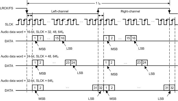
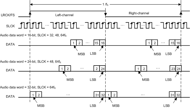
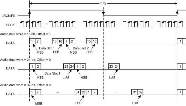
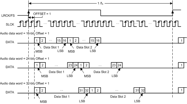
The serial audio interface port is a 3-wire serial port with the signals LRCK/FS (pin 25), SCLK (pin 23), and SDIN (pin 24). SCLK is the serial audio bit clock, used to clock the serial data present on SDIN into the serial shift register of the audio interface. Serial data is clocked into the TAS5756M device on the rising edge of SCLK.The LRCK/FS pin is the serial audio left/right word clock or frame sync when the device is operated in TDM Mode.
Table 7. TAS5756M device Audio Data Formats, Bit Depths and Clock Rates
| FORMAT | DATA BITS | MAXIMUM LRCK/FS FREQUENCY (kHz) | MCLK RATE (fS) | SCLK RATE (fS) |
|---|---|---|---|---|
| I2S/LJ/RJ | 32, 24, 20, 16 | Up to 192 | 128 to 3072 (≤ 50 MHz) | 64, 48, 32 |
| TDM/DSP | 32, 24, 20, 16 | Up to 48 | 128 to 3072 | 125, 256 |
| 96 | 128 to 512 | 125, 256 | ||
| 192 | 128, 192, 256 | 128 |
The TAS5756M device requires the synchronization of LRCK/FS and system clock, but does not need a specific phase relation between LRCK/FS and system clock.
If the relationship between LRCK/FS and system clock changes more than ±5 MCLK, internal operation is initialized within one sample period and analog outputs are forced to the bipolar zero level until re-synchronization between LRCK/FS and system clock is completed.
If the relationship between LRCK/FS and SCLK are invalid more than 4 LRCK/FS periods, internal operation is initialized within one sample period and analog outputs are forced to the bipolar zero level until re-synchronization between LRCK/FS and SCLK is completed.
8.3.3.5.1 Data Formats and Master/Slave Modes of Operation
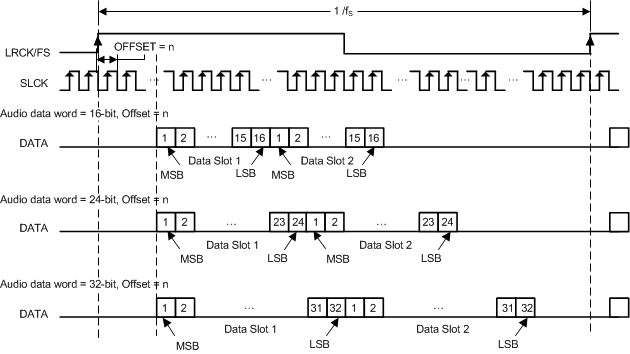
The TAS5756M device supports industry-standard audio data formats, including standard I2S and left-justified. Data formats are selected via Register (P0-R40). All formats require binary two's complement, MSB-first audio data; up to 32-bit audio data is accepted. The data formats are detailed in Figure 64 through Figure 69.
The TAS5756M device also supports right-justified and TDM/DSP data. I2S, LJ, RJ, and TDM/DSP are selected using Register (P0-R40). All formats require binary 2s complement, MSB-first audio data. Up to 32 bits are accepted. Default setting is I2S and 24 bit word length. The I2S slave timing is shown in .
shows a detailed timing diagram for the serial audio interface.
In addition to acting as a I2S slave, the TAS5756M device can act as an I2S master, by generating SCLK and LRCK/FS as outputs from the MCLK input. Table 8 lists the registers used to place the device into Master or Slave mode. Please refer to theSerial Audio Port Timing – Master Mode section for serial audio Interface timing requirements in Master Mode. For Slave Mode timing, please refer to to the Serial Audio Port Timing – Slave Mode section.
Table 8. I2S Master Mode Registers
| REGISTER | FUNCTION |
|---|---|
| P0-R9-B0, B4, and B5 | I2S Master mode select |
| P0-R32-B[6:0] | SCLK divider and LRCK/FS divider |
| P0-R33-B[7:0] |
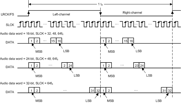 Figure 64. Left Justified Audio Data Format
8.3.3.6 Input Signal Sensing (Power-Save Mode)
The TAS5756M device has a zero-detect function. This function can be applied to both channels of data as an AND function or an OR function, via controls provided in the control port in P0-R65-B[2:1].Continuous Zero data cycles are counted by LRCK/FS, and the threshold of decision for analog mute can be set by P0-R59, B[6:4] for the data which is clocked in on the left frame of an I2S signal or Slot 1 of a TDM signal and P0-R59, B[2:0] for the data which is clocked in on the right frame of an I2S signal or Slot 2 of a TDM signal as shown in Table 10. Default values are 0 for both channels.
Table 9. Zero Detection Mode
| ATMUTECTL | VALUE | FUNCTION |
|---|---|---|
| Bit : 2 | 0 | Zero data triggers for the two channels for zero detection are ORed together. |
| 1 (Default) | Zero data triggers for the two channels for zero detection are ANDed together. | |
| Bit : 1 | 0 | Zero detection and analog mute are disabled for the data clocked in on the right frame of an I2S signal or Slot 2 of a TDM signal. |
| 1 (Default) | Zero detection analog mute are enabled for the data clocked in on the right frame of an I2S signal or Slot 2 of a TDM signal. | |
| Bit : 0 | 0 | Zero detection analog mute are disabled for the data clocked in on the left frame of an I2S signal or Slot 1 of a TDM signal. |
| 1 (Default) | Zero detection analog mute are enabled for the data clocked in on the left frame of an I2S signal or Slot 1 of a TDM signal. |
Table 10. Zero Data Detection Time
| ATMUTETIML OR ATMA | NUMBER OF LRCK/FS CYCLES | TIME at 48 kHz |
|---|---|---|
| 0 0 0 | 1024 | 21 ms |
| 0 0 1 | 5120 | 106 ms |
| 0 1 0 | 10240 | 213 ms |
| 0 1 1 | 25600 | 533 ms |
| 1 0 0 | 51200 | 1.066 secs |
| 1 0 1 | 102400 | 2.133 secs |
| 1 1 0 | 256000 | 5.333 secs |
| 1 1 1 | 512000 | 10.66 secs |
8.3.3.7 Serial Data Output
If it is supported by the HybridFlow in use, the TAS5756M device can present serial data on one of the three available hardware pins, GPIO0, GPIO1, or GPIO2. In a HybridFlow which supports serial data out, the serial data out origin can always be configured to come before the mini-DSP, by clearing the SDSL bit in P0-R7. This feature is used as a loop-back to check the integrity of the data transmission from the source to the TAS5756M device . In addition to the default loop-back mode, HybridFlows allows the SDOUT signal to originate from either a point after the processing or from some intermediary point within the HybridFlow. This option is accomplished by setting the SDSL bit in P0-R7. Figure 70 shows how to configure the origin of the serial data output signal.
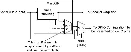 Figure 70. Serial Data Output Signal
Choosing the origin to be after all processing has been applied to the signal (i.e. before it is sent to the amplifier) is popular for sending a monitor signal back to a voice processing or echo-cancelling device elsewhere in the system. Other origins may configure the signal to originate after a subwoofer generation block, which sums in the inputs and applies a low-pass filter to create a mono, low-frequency signal. Please refer to the target HybridFlows for details regarding the options for the serial data output.
8.3.4 Modulation Scheme
8.3.4.1 BD-Modulation
The TAS5756M uses BD modulation. This modulation scheme allows operation without the classic LC output filter when the amp is driving an inductive load with short speaker wires. Each output is switching from 0 volts to the supply voltage PVDD. The SPK_OUTx+ and SPK_OUTx- are in phase with each other with no input signal so that there is little or no current in the speaker. The duty cycle of SPK_OUTx+ is greater than 50% and SPK_OUTx- is less than 50% for positive output voltages. The duty cycle of SPK_OUTx+ is less than 50% and SPK_OUTx- is greater than 50% for negative output voltages. The voltage across the load remains at 0 V throughout most of the switching period, reducing the switching current, which reduces any I2R losses in the load.
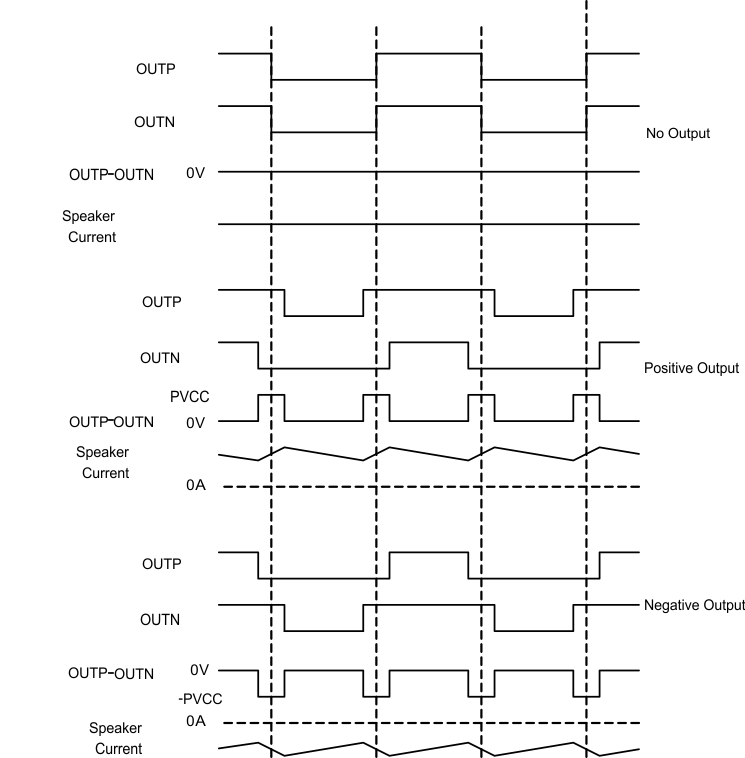 Figure 71. BD-Modulation
8.3.5 miniDSP Audio Processing Engine
The TAS5756M device integrates a highly efficient processing engine called a miniDSP. The miniDSP in the TAS5756M device uses a Hybrid architecture in which some processing blocks are built in ROM and other processing blocks are created in RAM via the PurePath™ Control Console GUI. This approach allows the flexibility of a fully-programmable device to be combined with the ease of use and rapid download time of a hard-coded ROM device.
8.3.5.1 HybridFlow Architecture
The Hybrid RAM and ROM Architecture allows the device to be highly flexible, but also easy to use. Unlike a device where all digital processing blocks are hard-coded in ROM, the hybrid RAM and ROM architecture allows a variety of processing blocks to be used in various combinations with various connectivity. These combinations of processing blocks are called HybridFlows.
HybridFlows are generated by combining a collection of processing blocks together in a targeted manner so that the device is well suited for a particular application or use case. Some HybridFlows are targeted for stereo applications, while others are targeted for mono, 1.1 (Bi-Amped), or 2.1 configurations.
It is important to note that the amount of processing which can be combined together into a given process flow is highly dependent on the sample rate of the audio signal which is being processed. For instance, an audio signal at 48 kHz can have much more processing applied than the same signal presented to the TAS5756M device at 192 kHz sample rate. For this reason, a HybridFlow which supports only up to 48 kHz sample rate cannot be used with a 192 kHz input signal.
8.3.5.2 Volume Control
8.3.5.2.1 Digital Volume Control
A basic digital volume control with range between 24 dB and 103 dB and mute is available on each channels by P0-R61-B[7:0] for SPK_OUTB± and P0-R62-B[7:0] for SPK_OUTA±. These volume controls all have 0.5 dB step programmability over most gain and attenuation ranges. Table 11 lists the detailed gain versus programmed setting for this basic volume control. Volume can be changed for both SPK_OUTB± and SPK_OUTA± at the same time or independently by P0-R61-B[1:0] . When B[1:0] set 00 (default), independent control is selected. When B[1:0] set 01, SPK_OUTA± accords with SPK_OUTB± volume. When B[1:0] set 10, SPK_OUTA± volume controls the volume for both channels. To set B[1:0] to 11 is prohibited.
Table 11. Digital Volume Control Settings
| GAIN SETTING | BINARY DATA | GAIN (dB) | COMMENTS |
|---|---|---|---|
| 0 | 0000-0000 | 24.0 | Positive maximum |
| 1 | 0000-0001 | 23.5 | |
| . . . |
. . . |
. . . |
|
| 46 | 0010-1110 | 1.0 | |
| 47 | 0010-1111 | 0.5 | |
| 48 | 0011-0000 | 0.0 | No attenuation (default) |
| 49 | 0011-0001 | –0.5 | |
| 50 | 0011-0010 | –1.0 | |
| 51 | 0011-0011 | –1.5 | |
| . . . |
. . . |
. . . |
|
| 253 | 1111-1101 | –102.5 | |
| 254 | 1111-1110 | –103 | Negative maximum |
| 255 | 1111-1111 | – |
Negative infinite (Mute) |
Ramp-up frequency and ramp-down frequency can be controlled by P0-R63, B[7:6] and B[3:2] as shown in Table 12. Also ramp-up step and ramp-down step can be controlled by P0-R63, B[5:4] and B[1:0] as shown in Table 13.
Table 12. Ramp Up or Down Frequency
| RAMP UP SPEED | EVERY N fS | COMMENTS | RAMP DOWN FREQUENCY | EVERY N fS | COMMENTS |
|---|---|---|---|---|---|
| 00 | 1 | Default | 00 | 1 | Default |
| 01 | 2 | 01 | 2 | ||
| 10 | 4 | 10 | 4 | ||
| 11 | Direct change | 11 | Direct change |
Table 13. Ramp Up or Down Step
| RAMP UP STEP | STEP dB | COMMENTS | RAMP DOWN STEP | STEP dB | COMMENTS |
|---|---|---|---|---|---|
| 00 | 4.0 | 00 | –4.0 | ||
| 01 | 2.0 | 01 | –2.0 | ||
| 10 | 1.0 | Default | 10 | –1.0 | Default |
| 11 | 0.5 | 11 | –0.5 |
8.3.5.2.1.1 Emergency Volume Ramp Down
Emergency ramp down of the volume by is provided for situations such as I2S clock error and power supply failure. Ramp-down speed is controlled by P0-R64-B[7:6]. Ramp-down step can be controlled by P0-R64-B[5:4]. Default is ramp-down by every fS cycle with –4dB step.
8.3.6 Adjustable Amplifier Gain and Switching Frequency Selection
The voltage divider between the GVDD_REG pin a the SPK_GAIN/FREQ pin is used to set the gain and switching frequency of the amplifier. Upon start-up of the device, the voltage presented on the SPK_GAIN/FREQ pin is digitized and then decoded into a 3-bit word which is interpreted inside the TAS5756M device to correspond to a given gain and switching frequency. In order to change the SPK_GAIN or switching frequency of the amplifier, the device must first be powered down, and then powered back back, with the new voltage level presented to the device on the SPK_GAIN/FREQ pin.
Because the amplifier adds gain to both the signal and the noise present in the audio signal, the lowest gain setting that can meet voltage-limited output power targets should be used. This ensures that the power target can be reached while minimizing the idle channel noise of the system. The switching frequency selection affects three important operating characteristics of the device. These are the power dissipation in the device, the power dissipation in the inductor, and the target output filter for the application.
Higher switching frequencies typically result in slightly higher power dissipation in the TAS5756M device and lower dissipation in the inductor in the system, due to decreased ripple current through the inductor and increased charging and discharging current in device and parasitic capacitances. Switching at the higher of the two available switching frequencies will result in lower overall dissipation in the system and lower operating temperature of the inductors. However, the thermally limited power output of the device may be decreased in this situation, because some of the TAS5756M device thermal headroom will be absorbed by the higher switching frequency. Conversely inductor heating can be reduced by using the higher switching frequency to reduce the ripple current.
Another advantage of increasing the switching frequency is that the higher frequency carrier signal can be filtered by an L-C filter with a higher corner frequency, leading to physically smaller components. Use the highest switching frequency that continues to meet the thermally limited power targets for the application. If thermal constraints require heat reduction in the TAS5756M device, use a lower switching rate.
The switching frequency of the speaker amplifier is dependent on an internal synchronizing signal, (fSYNC), which is synchronous with the sample rate. The rate of the synchronizing signal is also dependent on the sample rate. Refer to Table 14 below for details regarding how the sample rates correlate to the synchronizing signal.
Table 14. Sample Rates vs Synchronization Signal
| SAMPLE RATE [kHz] |
fSYNC
[kHz] |
|---|---|
| 8 | 96 |
| 16 | |
| 32 | |
| 48 | |
| 96 | |
| 192 | |
| 11.025 | 88.2 |
| 22.05 | |
| 44.1 | |
| 88.2 |
Table 15 summarizes the de-code of the voltage presented to the SPK_GAIN/FREQ pin. The voltage presented to the SPK_GAIN/FREQ pin is latched in upon startup of the device. Subsequent changes require power cycling the device. A gain setting of 20 dBV is recommended for nominal supply voltages of 13 V and lower, while a gain of 26 dBV is recommended for supply voltages up to 26.4 V. Table 15 shows the voltage required at the SPK_GAIN/FREQ pin for various gain and switching scenarios as well some example resistor values for meeting the voltage range requirements.
Table 15. Amplifier Switching Mode vs. SPK_GAIN/FREQ Voltage
8.3.7 Error Handling and Protection Suite
8.3.7.1 Device Overtemperature Protection
The TAS5756M device continuously monitors die temperature to ensure it does to exceed the OTETHRES level specified in the Recommended Operating Conditions table. If an OTE event occurs, the SPK_FAULT line is pulled low and out the SPK_OUTxx outputs transition to high impedance, signifying a fault. This is a non-latched error and will attempt to self clear after OTECLRTIME has passed.
8.3.7.2 SPK_OUTxx Overcurrent Protection
The TAS5756M device continuously monitors the output current of each amplifier output to ensure it does to exceed the OCETHRES level specified in the Recommended Operating Conditions table. If an OCE event occurs, the SPK_FAULT line is pulled low and the SPK_OUTxx outputs transition to high impedance, signifying a fault. This is a non-latched error and will attempt to self clear after OCECLRTIME has passed.
8.3.7.3 DC Offset Protection
If the TAS5756M device measures a DC offset in the output voltage, the SPK_FAULT line is pulled low and the SPK_OUTxx outputs transition to high impedance, signifying a fault. This latched error require the SPK_MUTE line to toggle to reset the error. Alternatively, pulling the MCLK, SCLK, or LRCK low causes a clock error, which also resets the device. Normal operation resumes by re-starting the stopped clock.
8.3.7.4 Internal VAVDD Undervoltage-Error Protection
The TAS5756M device internally monitors the AVDD net to protect against the AVDD supply dropping unexpectedly. To enable this feature, P1-R5-B0 is used.
8.3.7.5 Internal VPVDD Undervoltage-Error Protection
If the voltage presented on the PVDD supply drops below the UVETHRES(PVDD) value listed in the Recommended Operating Conditions table, the SPK_OUTxx outputs transition to high impedance. This is a self-clearing error, which means that once the PVDD level drops below the level listed in the Recommended Operating Conditions table, the device resumes normal operation.
8.3.7.6 Internal VPVDD Overvoltage-Error Protection
If the voltage presented on the PVDD supply exceeds the OVETHRES(PVDD) value listed in the Recommended Operating Conditions table, the SPK_OUTxx outputs will transition to high impedance. This is a self-clearing error, which means that once the PVDD level drops below the level listed in the Recommended Operating Conditions table, the device will resume normal operation. It is important to note that this voltage only protects up to the level described in the Recommended Operating Conditions table for the PVDD voltage. Exceeding this absolute maximum rating causes damage and possible device failure, because the levels exceed that which can be protected against by the OVE protection circuit.
8.3.7.7 External Undervoltage-Error Protection
The SPK_MUTE pin can also be used to monitor a system voltage, such as a LCD TV backlight, a battery pack in portable device, by using a voltage divider created with two resistors (see Figure 72).
- If the SPK_MUTE pin makes a transition from 1 to 0 over 6 ms or more, the device switches into external undervoltage protection mode. This mode uses two trigger levels.
- When the SPK_MUTE pin level reaches 2 V, soft mute process begins.
- When the SPK_MUTE pin level reaches 1.2 V, analog output mute engages, regardless of digital audio level, and analog output shutdown begins.
Figure 73 shows a timing diagram for external undervoltage error protection.
NOTE
The SPK_MUTE input pin voltage range is provided in the Recommended Operating Conditions table. The ratio of external resistors must produce a voltage within this input range. Any increase in power supply (such as power supply positive noise or ripple) can pull the SPK_MUTE pin higher than that the level specified in the Recommended Operating Conditions table, potentially causing damage to or failure of the device. Therefore, it is imperative that any monitored voltage (including all ripple, power supply variation, resistor divider variation, transient spikes, and others) is scaled by the resistor divider network to never drive the voltage on the SPK_MUTE pin higher than the maximum level specified in the Recommended Operating Conditions table.
When the divider is set correctly, any DC voltage can be monitored. Figure 72 shows a 12-V example of how the SPK_MUTE is used for external undervoltage error protection.
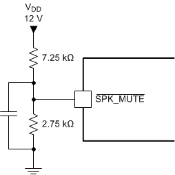 Figure 72. SPK_MUTE Used in External Undervoltage Error Protection
 Figure 73. SPK_MUTE Timing for External Undervoltage Error Protection
8.3.7.8 Internal Clock Error Notification (CLKE)
8.3.8 GPIO Port and Hardware Control Pins
The TAS5756M device includes a versatile GPIO port, allowing signals to be passed from the system to the device or sent out of the device to the system. There are three GPIO pins available for use. These pins can be used for advanced clocking features, to pass internal signals to the system or accept signals from the system for use inside the device by a HybridFlow, or simply to monitor the status of an external signal via I2C. The GPIO port requires some configuration in the control port. This configuration is detailed in Figure 74.
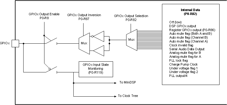 Figure 74. GPIO Port
In addition to the dynamic controls which can be implemented with the GPIO port, each HybridFlow uses the GPIO port as required. In some HybridFlows, a GPIO is used to present an internal serial audio data signal to a system controller. In others, the status of a GPIO pin is monitored and the status of that pin is used to adjust the audio processing applied to the signal. Refer to each HybridFlow for specifics regarding how the GPIO port is used. GPIOs which have been allocated to a function in a HybridFlow can be reassigned using the same controls as those listed in Figure 74. However, they no longer serve the purpose intended by the design of the HybridFlow.
8.3.9 I2C Communication Port
The TAS5756M device supports the I2C serial bus and the data transmission protocol for standard and fast mode as a slave device. Because the TAS5756M register map spans several pages, it is be necessary to change from page to page before writing individual register bits or bytes. This is accomplished via register 0 on each page. This register value selects the register page, from 0 to 255.
8.3.9.1 Slave Address
Table 16. I2C Slave Address
| MSB | LSB | ||||||
| 1 | 0 | 0 | 1 | 1 | ADR2 | ADR1 | R/ W |
The TAS5756M device has 7 bits for its own slave address. The first five bits (MSBs) of the slave address are factory preset to 10011 (0x9x). The next two bits of the address byte are the device select bits which can be user-defined by the ADR1 and ADR0 terminals. A maximum of four devices can be connected on the same bus at one time. This gives a range of 0x98, 0x9A, 0x9C and 0x9E, as detailed below. Each TAS5756M device responds when it receives its own slave address.
Table 17. I2C Address Configuration via ADR0 and ADR1 Pins
| ADR1 | ADR0 | I2C SLAVE ADDRESS [R/W] |
|---|---|---|
| 0 | 0 | 0x99/0x98 |
| 0 | 1 | 0x9B/0x9A |
| 1 | 0 | 0x9D/0x9C |
| 1 | 1 | 0x9F/0x9E |
8.3.9.2 Register Address Auto-Increment Mode
 Figure 75. Auto Increment Mode
Auto-increment mode allows multiple sequential register locations to be written to or read back in a single operation, and is especially useful for block write and read operations.
8.3.9.3 Packet Protocol
A master device must control packet protocol, which consists of start condition, slave address, read/write bit, data if write or acknowledge if read, and stop condition. The TAS5756M device supports only slave receivers and slave transmitters.
 Figure 76. Packet Protocol
Table 18. Write Operation - Basic I2C Framework
| Transmitter | M | M | M | S | M | S | M | S | S | M | |
| Data Type | St | slave address | R/ | ACK | DATA | ACK | DATA | ACK | ACK | Sp |
Table 19. Read Operation - Basic I2C Framework
| Transmitter | M | M | M | S | S | M | S | M | M | M | |
| Data Type | St | slave address | R/ | ACK | DATA | ACK | DATA | ACK | NACK | Sp |
M = Master Device; S = Slave Device; St = Start Condition Sp = Stop Condition
8.3.9.4 Write Register
A master can write to any TAS5756M device registers using single or multiple accesses. The master sends a TAS5756M device slave address with a write bit, a register address with auto-increment bit, and the data. If auto-increment is enabled, the address is that of the starting register, followed by the data to be transferred. When the data is received properly, the index register is incremented by 1 automatically. When the index register reaches 0x7F, the next value is 0x0. Table 20 shows the write operation.
Table 20. Write Operation
| Transmitter | M | M | M | S | M | S | M | S | M | S | S | M | ||
| Data Type | St | slave addr | W | ACK | inc | reg addr | ACK | write data 1 | ACK | write data 2 | ACK | ACK | Sp | |
M = Master Device; S = Slave Device; St = Start Condition Sp = Stop Condition; W = Write; ACK = Acknowledge
8.3.9.5 Read Register
A master can read the TAS5756M device register. The value of the register address is stored in an indirect index register in advance. The master sends a TAS5756M device slave address with a read bit after storing the register address. Then the TAS5756M device transfers the data which the index register points to. When auto-increment is enabled, the index register is incremented by 1 automatically. When the index register reaches 0x7F, the next value is 0x0. Table 21 lists the read operation.
Table 21. Read Operation
| Transmitter | M | M | M | S | M | S | M | M | M | S | S | M | M | M | ||
| Data Type | St | slave addr | W | ACK | inc | reg addr | ACK | Sr | slave addr | R | ACK | data | ACK | NACK | Sp | |
M = Master Device; S = Slave Device; St = Start Condition; Sr = Repeated start condition; Sp = Stop Condition; W = Write; R = Read; NACK = Not acknowledge
8.4 Device Functional Modes
Because the TAS5756M device is a highly configurable device, numerous modes of operation can exist for the device. For the sake of succinct documentation, these modes are divided into two modes:
- Fundamental operating modes
- Secondary usage modes
Fundamental operating modes are the primary modes of operation that affect the major operational characteristics of the device. These are the most basic configurations that are chosen to ensure compatibility with the intended application or the other components that interact with the device in the final system. Some examples of these are the communication protocol used by the control port, the output configuration of the amplifier, or the Master/Slave clocking configuration.
The fundamental operating modes are described starting in the Serial Audio Port Operating Modes section.
Secondary usage modes are best described as modes of operation that are used after the fundamental operating modes are chosen to fine tune how the device operates within a given system. These secondary usage modes may include selecting between left justified and right justified Serial Audio Port data formats, or enabling some slight gain/attenuation within the DAC path. Secondary usage modes are accomplished through manipulation of the registers and controls in the I2C control port. Those modes of operation are described in their respective register/bit descriptions and, to avoid redundancy, are not included in this section.
8.4.1 Serial Audio Port Operating Modes
The serial audio port in the TAS5756M device supports industry-standard audio data formats, including I2S, Time Division Multiplexing (TDM), Left-Justified (LJ), and Right-Justified (RJ) formats. To select the data format that will be used with the device, controls are provided on P0-R40. The timing diagrams for the serial audio port are shown in theSerial Audio Port Timing – Slave Mode section, and the data formats are shown in the Serial Audio Port – Data Formats and Bit Depths section.
8.4.2 Communication Port Operating Modes
The TAS5756M device is configured via an I2C communication port. The device does not support a hardware only mode of operation, nor Serial Peripheral Interface (SPI) communication. The I2C Communication Protocol is detailed in theI2C Communication Port section. The I2C timing requirements are described in the I2C Bus Timing – Standard and I2C Bus Timing – Fast sections.
8.4.3 Audio Processing Modes via HybridFlow Audio Processing
The TAS5756M device can be configured to include several different audio processing features through the use of pre-defined DSP loads called HybridFlows. These HybridFlows have been created and tested to be application focused. This approach results in a device which offers the flexibility of a programmable device with the ease-of-use and fast download time of a fixed function device. The HybridFlows are selected and downloaded using the PurePath™ ControlConsole software. .
8.4.4 Speaker Amplifier Operating Modes
The TAS5756M device can be used in three different amplifier configurations:
- Stereo Mode
- Mono Mode
- Bi-Amp Mode
8.4.4.1 Stereo Mode
The familiar stereo mode of operation uses the TAS5756M device to amplify two independent signals, which represent the left and right portions of a stereo signal. These amplified left and right audio signals are presented on differential output pairs shown as SPK_OUTA± and SPK_OUTB±. The routing of the audio data which is presented on the SPK_OUTxx outputs can be changed according to the HybridFlow which is used and the configuration of registers P0-R42-B[5:4] and P0-R42-B[1:0]. This mode of operation is shown in Figure 79.
By default, the TAS5756M device is configured to output the Right frame of a I2S input on the Channel A output and the left frame on the Channel B output.
8.4.4.2 Mono Mode
This mode of operation is used to describe operation in which the two outputs of the device are placed in parallel with one another to increase the power sourcing capabilities of the device.
On the output side of the TAS5756M device, the summation of the devices can be done before the filter in a configuration called Pre-Filter Parallel Bridge Tied Load (PBTL). However, it is sometimes preferable to merge the two outputs together after the inductor portion of the output filter. Doing so does require two additional inductors, but allows smaller, less expensive inductors to be used because the current is divided between the two inductors. This is called Post-Filter PBTL. Both variants of mono operation are shown in Figure 77 and Figure 78.
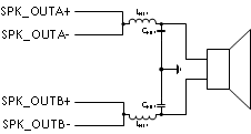 Figure 77. Pre-Filter PBTL
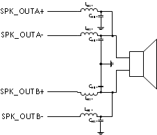 Figure 78. Post-Filter PBTL
On the input side of the TAS5756M device, the input signal to the mono amplifier can be selected from the any slot in a TDM stream or the left or right frame from an I2S, LJ, or RJ signal. It can also be configured to amplify some mixture of two signals, as in the case of a subwoofer channel which mixes the left and right channel together and sends it through a low-pass filter to create a mono, low-frequency signal.
This mode of operation is shown in the Mono (PBTL) Systems section.
8.4.4.3 Bi-Amp Mode
Bi-Amp mode, sometimes also referred to as 1.1 Mode uses a two channel device (such as the TAS5756M device ) to amplify two different frequency regions of the same signal for a two-way speaker. This is most often used in a single active speaker, where one channel of the amplifier is use to drive the high frequency transducer and one channel is used to drive the low-frequency transducer. To operate in Bi-Amped Mode or 1.1 Mode, an appropriate HybridFlow must be selected, because the frequency separation and audio processing must occur in the DSP. This mode of operation is shown in the 1.1 (Dual BTL, Bi-Amped) Systems section.
8.4.4.4 Master and Slave Mode Clocking for Digital Serial Audio Port
The digital audio serial port in the TAS5756M device can be configured to receive its clocks from another device as a serial audio slave device. This mode of operation is described in the Clock Slave Mode with SLCK PLL to Generate Internal Clocks (3-Wire PCM) section. If there no system processor available to provide the audio clocks, the TAS5756M device can be placed into Master Mode. In this mode, the TAS5756M device provides the clocks to the other audio devices in the system. For more details regarding the Master and Slave mode operation within the TAS5756M device, see the Serial Audio Port Operating Modes section.