SLASEV8 December 2020 TAS5822M
PRODUCTION DATA
- 1 Features
- 2 Applications
- 3 Description
- 4 Revision History
- 5 Pin Configuration and Functions
- 6 Specifications
-
7 Detailed Description
- 7.1 Overview
- 7.2 Functional Block Diagram
- 7.3 Feature Description
- 7.4 Device Functional Modes
- 7.5 Programming and Control
- 7.6 Register Maps
- 8 Application and Implementation
- 9 Power Supply Recommendations
- 10Layout
- 11Device and Documentation Support
- 12Mechanical, Packaging, and Orderable Information
Package Options
Mechanical Data (Package|Pins)
- DCP|38
Thermal pad, mechanical data (Package|Pins)
- DCP|38
Orderable Information
5 Pin Configuration and Functions
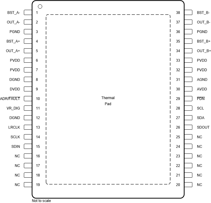
 Figure 5-1 DCP
Package,38-Pin TSSOP, Top
View
Figure 5-1 DCP
Package,38-Pin TSSOP, Top
ViewTable 5-1 Pin Functions
| PIN | TYPE(1) | DESCRIPTION | |
|---|---|---|---|
| NAME | NO. | ||
| DGND | 8,12 | G | Digital ground |
| DVDD | 9 | P | 3.3-V or 1.8-V digital power supply |
| VR_DIG | 11 | P | Internally regulated 1.5-V digital supply voltage. This pin must not be used to drive external devices |
| ADR/ FAULT | 10 | DIO | Different I2 C device address can be set by selecting different pull up resistor to DVDD, see Table 4 for details. This pin can be programed by writing 1 to a register bit after Power up bit. In this mode, the ADR/ FAULT Is redefined as FAULT,go to Page 0, Book 0, set register 0x61 = 0x0b first, then set register 0x60 = 0x01 |
| LRCLK | 13 | DI | Word select clock for the digital signal that is active on the serial port's input data line. In I2S, LJ and RJ, this corresponds to the left channel and right channel boundary. In TDM mode, this corresponds to the frame sync boundary. |
| SCLK | 14 | DI | Bit clock for the digital signal that is active on the input data line of the serial data port. |
| SDIN | 15 | DI | Data line to the serial data port |
| SDOUT | 26 | DO | Serial Audio data output, the source data can select as Pre-DSP or Post DSP |
| SDA | 27 | DI/O | I2C serial control data interface input/output |
| SCL | 28 | DI | I2C serial control clock input |
| PDN | 29 | DI | Power Down, active-low. PDN place the amplifier in Shutdown, turn off all internal regulators. |
| AVDD | 30 | P | Internally regulated 5-V analog supply voltage. This pin must not be used to drive external devices |
| AGND | 31 | G | Analog ground |
| PVDD | 6 | P | PVDD voltage input |
| 7 | P | ||
| 32 | P | ||
| 33 | P | ||
| PGND | 3 | G | Ground reference for power device circuitry. Connect this pin to system ground. |
| 36 | G | ||
| OUT_A+ | 5 | O | Positive pin for differential speaker amplifier output A+ |
| BST_A+ | 4 | P | Connection point for the OUT_A+ bootstrap capacitor which is used to create a power supply for the high-side gate drive for OUT_A+ |
| OUT_A- | 2 | O | Negative pin for differential speaker amplifier output A- |
| BST_A- | 1 | P | Connection point for the OUT_A- bootstrap capacitor which is used to create a power supply for the high-side gate drive for OUT_A- |
| BST_B- | 38 | P | Connection point for the OUT_B- bootstrap capacitor which is used to create a power supply for the high-side gate drive for OUT_B- |
| OUT_B- | 37 | O | Negative pin for differential speaker amplifier output B |
| BST_B+ | 35 | P | Connection point for the OUT_B+ bootstrap capacitor which is used to create a power supply for the high-side gate drive for OUT_B+ |
| OUT_B+ | 34 | O | Positive pin for differential speaker amplifier output B+ |
| NC | 18 | - | No Connect Pin. Can be shorted to PVDD or shorted to GND or left open. |
| NC | 19 | - | No Connect Pin. Can be shorted to PVDD or shorted to GND or left open. |
| NC | 20 | - | No Connect Pin. Can be shorted to PVDD or shorted to GND or left open. |
| NC | 21 | - | No Connect Pin. Can be shorted to PVDD or shorted to GND or left open. |
| NC | 17 | - | No Connect Pin. Can be shorted to PVDD or shorted to GND or left open. |
| NC | 16 | - | No Connect Pin. Can be shorted to PVDD or shorted to GND or left open. |
| NC | 22 | - | No Connect Pin. Can be shorted to PVDD or shorted to GND or left open. |
| NC | 25 | - | No Connect Pin. Can be shorted to PVDD or shorted to GND or left open. |
| NC | 23 | - | No Connect Pin. Can be shorted to PVDD or shorted to GND or left open. |
| NC | 24 | - | No Connect Pin. Can be shorted to PVDD or shorted to GND or left open. |
| PowerPAD™ | G | Connect to the system Ground | |
(1) AI = Analog input, AO = Analog output, DI = Digital Input, DO =
Digital Output, DI/O = Digital Bi-directional (input and output), P = Power, G =
Ground (0 V)