SCPS234A September 2016 – February 2023 TCA6408A-Q1
PRODUCTION DATA
- 1 Features
- 2 Applications
- 3 Description
- 4 Revision History
- 5 Pin Configuration and Functions
- 6 Specifications
- 7 Parameter Measurement Information
- 8 Detailed Description
- 9 Application and Implementation
- 10Device and Documentation Support
- 11Support Resources
- 12Mechanical, Packaging, and Orderable Information
Package Options
Mechanical Data (Package|Pins)
- PW|16
Thermal pad, mechanical data (Package|Pins)
Orderable Information
9.2.1.1 Calculating Junction Temperature and Power Dissipation
When designing with the TCA6408A-Q1, it is important that the Section 6.3 not be violated. Many of the parameters of this device are rated based on junction temperature. So junction temperature must be calculated in order to verify that safe operation of the device is met. The basic equation for junction temperature is shown in Equation 1.
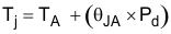
θJA is the standard junction to ambient thermal resistance measurement of the package, as seen in Section 6.4 table. Pd is the total power dissipation of the device, and the approximation is shown in Equation 2.

Equation 2 is the approximation of power dissipation in the device. The equation is the static power plus the summation of power dissipated by each port (with a different equation based on if the port is outputting high, or outputting low. If the port is set as an input, then power dissipation is the input leakage of the pin multiplied by the voltage on the pin). Note that this ignores power dissipation in the INT and SDA pins, assuming these transients to be small. They can easily be included in the power dissipation calculation by using Equation 3 to calculate the power dissipation in INT or SDA while they are pulling low, and this gives maximum power dissipation.
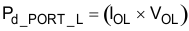
Equation 3 shows the power dissipation for a single port which is set to output low. The power dissipated by the port is the VOL of the port multiplied by the current it is sinking.
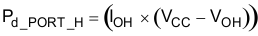
Equation 4 shows the power dissipation for a single port which is set to output high. The power dissipated by the port is the current sourced by the port multiplied by the voltage drop across the device (difference between VCC and the output voltage).