SCPS245C December 2012 – December 2018 TCA9517A
PRODUCTION DATA.
- 1 Features
- 2 Applications
- 3 Description
- 4 Revision History
- 5 Description (continued)
- 6 Pin Configuration and Functions
- 7 Specifications
- 8 Parameter Measurement Information
- 9 Detailed Description
- 10Application and Implementation
- 11Power Supply Recommendations
- 12Layout
- 13Device and Documentation Support
- 14Mechanical, Packaging, and Orderable Information
Package Options
Mechanical Data (Package|Pins)
- DGK|8
Thermal pad, mechanical data (Package|Pins)
- DGK|8
Orderable Information
8 Parameter Measurement Information

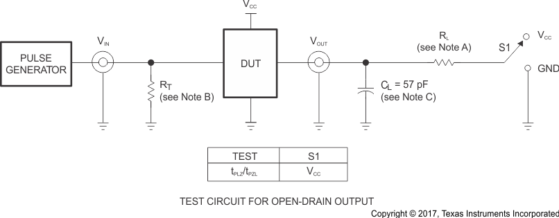
A. RL = 167 Ω (0.9 V to 2.7 V) and RL = 450 Ω (3.0 V to 5.5 V) on the A side and 1.35 kΩ on the B-side
B. RT termination resistance should be equal to ZOUT of pulse generators.
C. CL includes probe and jig capacitance.
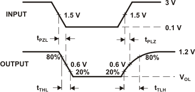
D. All input pulses are supplied by generators having the following characteristics: PRR ≤ 10 MHz, ZO = 50 Ω, slew rate ≥ 1 V/ns.
E. The outputs are measured one at a time, with one transition per measurement.
F. tPLH and tPHL are the same as tpd.
G. tPLZ and tPHZ are the same as tdis.
H. tPZL and tPZH are the same as ten.
Figure 3. Test Circuit  Figure 4. Waveform 1 – Propagation Delay and Transition Times for B-side to A-side
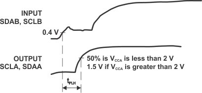
  Figure 6. Waveform 3 – Propagation Delay for B-side to A-side
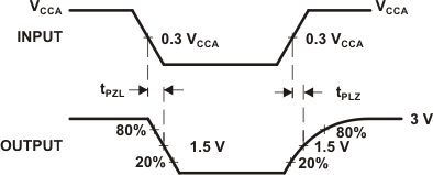
  Figure 5. Waveform 2 – Propagation Delay and Transition Times for A-side to B-side