SCPS280A November   2022  – November 2023 TCAL9538

PRODUCTION DATA  

  1.   1
  2. Features
  3. Applications
  4. Description
  5. Pin Configuration and Functions
  6. Specifications
    1. 5.1 Absolute Maximum Ratings
    2. 5.2 ESD Ratings
    3. 5.3 Recommended Operating Conditions
    4. 5.4 Thermal Information
    5. 5.5 Electrical Characteristics
    6. 5.6 Timing Requirements
    7. 5.7 I2C Bus Timing Requirements
    8. 5.8 Switching Characteristics
    9. 5.9 Typical Characteristics
  7. Parameter Measurement Information
  8. Detailed Description
    1. 7.1 Overview
    2. 7.2 Functional Block Diagrams
    3. 7.3 Feature Description
      1. 7.3.1 I/O Port
      2. 7.3.2 Adjustable Output Drive Strength
      3. 7.3.3 Interrupt Output (INT)
      4. 7.3.4 Reset Input (RESET)
      5. 7.3.5 Software Reset Call
    4. 7.4 Device Functional Modes
      1. 7.4.1 Power-On Reset
    5. 7.5 Programming
      1. 7.5.1 I2C Interface
    6. 7.6 Register Maps
      1. 7.6.1 Device Address
      2. 7.6.2 Control Register and Command Byte
      3. 7.6.3 Register Descriptions
      4. 7.6.4 Bus Transactions
        1. 7.6.4.1 Writes
        2. 7.6.4.2 Reads
  9. Application and Implementation
    1. 8.1 Application Information
    2. 8.2 Typical Application
      1. 8.2.1 Design Requirements
      2. 8.2.2 Detailed Design Procedure
        1. 8.2.2.1 Minimizing ICC When I/Os Control LEDs
      3. 8.2.3 Application Curves
    3. 8.3 Power Supply Recommendations
      1. 8.3.1 Power-On Reset Requirements
    4. 8.4 Layout
      1. 8.4.1 Layout Guidelines
      2. 8.4.2 Layout Example
  10. Device and Documentation Support
    1. 9.1 Receiving Notification of Documentation Updates
    2. 9.2 Support Resources
    3. 9.3 Trademarks
    4. 9.4 Electrostatic Discharge Caution
    5. 9.5 Glossary
  11. 10Revision History
  12. 11Mechanical, Packaging, and Orderable Information

Package Options

Refer to the PDF data sheet for device specific package drawings

Mechanical Data (Package|Pins)
  • PW|16
  • DTU|16
  • RSV|16
Thermal pad, mechanical data (Package|Pins)
Orderable Information

Detailed Design Procedure

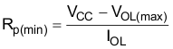
The pull-up resistors, RP, for the SCL and SDA lines need to be selected appropriately and take into consideration the total capacitance of all targets on the I2C bus. The minimum pull-up resistance is a function of VCC, VOL,(max), and IOL:

Equation 1. GUID-DD6FD861-B884-4ED8-BFC3-8865FCBAEA66-low.gif

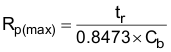
The maximum pull-up resistance is a function of the maximum rise time, tr (120 ns for fast-mode-plus operation, fSCL = 1 MHz) and bus capacitance, Cb:

Equation 2. GUID-D69A514A-196C-4378-BA0C-161D7A3FE943-low.gif

The maximum bus capacitance for an I2C bus must not exceed 400 pF for standard-mode or fast-mode operation, or 550 pF for fast-mode-plus. The bus capacitance can be approximated by adding the capacitance of the TCAL9538, Ci for SCL, or Cio for SDA. Plus the capacitance of wires, connections, traces, and the capacitance of additional targets on the bus.