SNAS648C October   2014  – February 2023 TDC1000

PRODUCTION DATA  

  1. Features
  2. Applications
  3. Description
  4. Revision History
  5. Pin Configuration and Functions
  6. Specifications
    1. 6.1 Absolute Maximum Ratings
    2. 6.2 ESD Ratings
    3. 6.3 Recommended Operating Conditions
    4. 6.4 Thermal Information (1)
    5. 6.5 Electrical Characteristics
    6. 6.6 Timing Requirements
    7. 6.7 Switching Characteristics
    8. 6.8 Typical Characteristics
  7. Parameter Measurement Information
  8. Detailed Description
    1. 8.1 Overview
    2. 8.2 Functional Block Diagram
    3. 8.3 Feature Description
      1. 8.3.1 Transmitter Signal Path
      2. 8.3.2 Receiver Signal Path
      3. 8.3.3 Low Noise Amplifier (LNA)
      4. 8.3.4 Programmable Gain Amplifier (PGA)
      5. 8.3.5 Receiver Filters
      6. 8.3.6 Comparators for STOP Pulse Generation
        1. 8.3.6.1 Threshold Detector and DAC
        2. 8.3.6.2 Zero-Cross Detect Comparator
        3. 8.3.6.3 Event Manager
      7. 8.3.7 Common-Mode Buffer (VCOM)
      8. 8.3.8 Temperature Sensor
        1. 8.3.8.1 Temperature Measurement With Multiple RTDs
        2. 8.3.8.2 Temperature Measurement With a Single RTD
    4. 8.4 Device Functional Modes
      1. 8.4.1 Time-of-Flight Measurement Mode
        1. 8.4.1.1 Mode 0
        2. 8.4.1.2 Mode 1
        3. 8.4.1.3 Mode 2
      2. 8.4.2 State Machine
      3. 8.4.3 TRANSMIT Operation
        1. 8.4.3.1 Transmission Pulse Count
        2. 8.4.3.2 TX 180° Pulse Shift
        3. 8.4.3.3 Transmitter Damping
      4. 8.4.4 RECEIVE Operation
        1. 8.4.4.1 Single Echo Receive Mode
        2. 8.4.4.2 Multiple Echo Receive Mode
      5. 8.4.5 Timing
        1. 8.4.5.1 Timing Control and Frequency Scaling (CLKIN)
        2. 8.4.5.2 TX/RX Measurement Sequencing and Timing
      6. 8.4.6 Time-of-Flight (TOF) Control
        1. 8.4.6.1 Short TOF Measurement
        2. 8.4.6.2 Standard TOF Measurement
        3. 8.4.6.3 Standard TOF Measurement With Power Blanking
        4. 8.4.6.4 Common-Mode Reference Settling Time
        5. 8.4.6.5 TOF Measurement Interval
      7. 8.4.7 Averaging and Channel Selection
      8. 8.4.8 Error Reporting
    5. 8.5 Programming
      1. 8.5.1 Serial Peripheral Interface (SPI)
        1. 8.5.1.1 Chip Select Bar (CSB)
        2. 8.5.1.2 Serial Clock (SCLK)
        3. 8.5.1.3 Serial Data Input (SDI)
        4. 8.5.1.4 Serial Data Output (SDO)
    6. 8.6 Register Maps
  9. Application and Implementation
    1. 9.1 Application Information
    2. 9.2 Typical Applications
      1. 9.2.1 Level and Fluid Identification Measurements
        1. 9.2.1.1 Design Requirements
        2. 9.2.1.2 Detailed Design Procedure
          1. 9.2.1.2.1 Level Measurements
          2. 9.2.1.2.2 Fluid Identification
        3. 9.2.1.3 Application Curves
      2. 9.2.2 Water Flow Metering
        1. 9.2.2.1 Design Requirements
        2. 9.2.2.2 Detailed Design Procedure
          1. 9.2.2.2.1 Regulations and Accuracy
          2. 9.2.2.2.2 Transit-Time in Ultrasonic Flow Meters
          3. 9.2.2.2.3 ΔTOF Accuracy Requirement Calculation
          4. 9.2.2.2.4 Operation
        3. 9.2.2.3 Application Curves
    3. 9.3 Power Supply Recommendations
    4. 9.4 Layout
      1. 9.4.1 Layout Guidelines
      2. 9.4.2 Layout Example
  10. 10Device and Documentation Support
    1. 10.1 Device Support
      1. 10.1.1 Development Support
    2. 10.2 Receiving Notification of Documentation Updates
    3. 10.3 Support Resources
    4. 10.4 Trademarks
    5. 10.5 Electrostatic Discharge Caution
    6. 10.6 Glossary
  11. 11Mechanical, Packaging, and Orderable Information

Package Options

Mechanical Data (Package|Pins)
Thermal pad, mechanical data (Package|Pins)
Orderable Information

Event Manager

The event manager is a digital state machine in the STOP pulse generation circuit of the TDC1000. The event manager controls the maximum number of STOP pulses to generate on the STOP pin and the receive mode for the STOP pulse generation. The number of STOP pulses is configured in the NUM_RX field in the CONFIG_1 register. The receive mode is selected in the RECEIVE_MODE bit of the CONFIG_4 register. See sections GUID-2034B423-2789-4CE3-9084-D9E69B654791.html#TITLE-SNAS648SNAS6489609 and GUID-04507CCD-73B6-4DAC-96E4-9F68454CABBC.html#TITLE-SNAS648SNAS6484838 for details about the receiver modes of the TDC1000.

#SNAS648960 shows an example for NUM_RX = 2h and RECEIVE_MODE = 0. When the echo signal amplitude exceeds values smaller than VTHLD, the threshold detect comparator indicates to the event manager to qualify the next zero-cross event as valid. When the qualified zero-cross is detected by the zero-cross detect comparator, the event manager passes the pulse to the STOP pin until the number of receive events programmed in NUM_RX is reached.
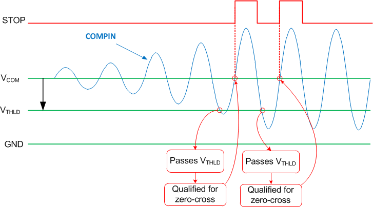
GUID-1AFF1ADA-1B1F-4334-B8A0-4006612375D3-low.gifFigure 8-8 Signal Qualification, Zero-Cross Detection and STOP Pulse Generation