SBOS932C January   2020  – March 2021 THP210

PRODUCTION DATA  

  1. Features
  2. Applications
  3. Description
  4. Revision History
  5. Pin Configuration and Functions
  6. Specifications
    1. 6.1 Absolute Maximum Ratings
    2. 6.2 ESD Ratings
    3. 6.3 Recommended Operating Conditions
    4. 6.4 Thermal Information
    5. 6.5 Electrical Characteristics
    6. 6.6 Typical Characteristics
  7. Parameter Measurement Information
    1. 7.1 Characterization Configuration
  8. Detailed Description
    1. 8.1 Overview
    2. 8.2 Functional Block Diagram
    3. 8.3 Feature Description
      1. 8.3.1 Super-Beta Input Bipolar Transistors
      2. 8.3.2 Power Down
      3. 8.3.3 Flexible Gain Setting
      4. 8.3.4 Amplifier Overload Power Limit
      5. 8.3.5 Unity Gain Stability
    4. 8.4 Device Functional Modes
  9. Application and Implementation
    1. 9.1 Application Information
      1. 9.1.1 I/O Headroom Considerations
      2. 9.1.2 DC Precision Analysis
        1. 9.1.2.1 DC Error Voltage at Room Temperature
        2. 9.1.2.2 DC Error Voltage Over Temperature
      3. 9.1.3 Noise Analysis
      4. 9.1.4 Mismatch of External Feedback Network
      5. 9.1.5 Operating the Power-Down Feature
      6. 9.1.6 Driving Capacitive Loads
      7. 9.1.7 Driving Differential ADCs
        1. 9.1.7.1 RC Filter Selection (Charge Kickback Filter)
        2. 9.1.7.2 Settling Time Driving the ADC Sample-and-Hold Operating Behavior
        3. 9.1.7.3 THD Performance
    2. 9.2 Typical Applications
      1. 9.2.1 MFB Filter
        1. 9.2.1.1 Design Requirements
        2. 9.2.1.2 Detailed Design Procedure
        3. 9.2.1.3 Application Curve
      2. 9.2.2 ADS891x With Single-Ended RC Filter Stage
        1. 9.2.2.1 Design Requirements
          1. 9.2.2.1.1 Measurement Results
      3. 9.2.3 Attenuation Configuration Drives the ADS8912B
        1. 9.2.3.1 Design Requirements
          1. 9.2.3.1.1 Measurement Results
  10. 10Power Supply Recommendations
  11. 11Layout
    1. 11.1 Layout Guidelines
      1. 11.1.1 Board Layout Recommendations
    2. 11.2 Layout Example
  12. 12Device and Documentation Support
    1. 12.1 Device Support
      1. 12.1.1 Development Support
    2. 12.2 Documentation Support
      1. 12.2.1 Related Documentation
    3. 12.3 Receiving Notification of Documentation Updates
    4. 12.4 Support Resources
    5. 12.5 Trademarks
    6. 12.6 Electrostatic Discharge Caution
    7. 12.7 Glossary
  13. 13Mechanical, Packaging, and Orderable Information

Package Options

Mechanical Data (Package|Pins)
Thermal pad, mechanical data (Package|Pins)
Orderable Information

Description

The THP210 is an ultra-low-offset, low-noise, high-voltage, precision, fully differential amplifier that easily filters and drives fully differential signal chains. The THP210 is also used to convert single-ended sources to differential outputs as required by high-resolution analog-to-digital converters (ADCs). Designed for exceptional offset, low noise and THD, the bipolar super-beta inputs yield a very-low noise figure at very-low quiescent current and input bias current. This device is designed for signal conditioning circuits where low power offset and power consumption are required, along with excellent signal-to-noise ratio (SNR).

The THP210 features high-voltage supply capability, allowing for supply voltages up to ±18 V. This capability allows high-voltage differential signal chains to benefit from the improved headroom and dynamic range without adding separate amplifiers for each polarity of the differential signal. Very-low voltage and current noise enables the THP210 for use in high-gain configurations with minimal impact to the signal fidelity.

Device Information(1)
PART NUMBER PACKAGE BODY SIZE (NOM)
THP210 VSSOP (8) 3.00 mm × 3.00 mm
SOIC (8) 4.90 mm x 3.91 mm
For all available packages, see the package option addendum at the end of the datasheet.


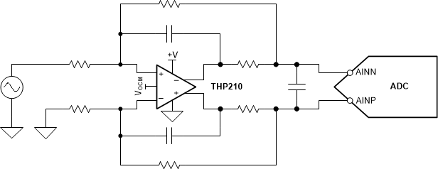
GUID-28A3231B-EBAA-4ADC-9A3E-211292821908-low.gifPrecision, Low-Noise, Low-Power, Fully-Differential Amplifier Gain Block and Interface
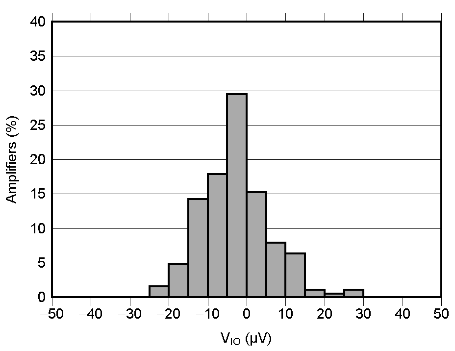
GUID-99EBC41D-4832-4E4B-9F2A-7AE5D94E3DEB-low.gifLow Input Voltage Offset