SBOS875C August 2017 – February 2023 THS3491
PRODUCTION DATA
- 1 Features
- 2 Applications
- 3 Description
- 4 Revision History
- 5 Device Comparison Table
- 6 Pin Configuration and Functions
- 7 Bare Die Information
- 8 Specifications
- 9 Detailed Description
- 10Application and Implementation
- 11Device and Documentation Support
- 12Mechanical, Packaging, and Orderable Information
Package Options
Mechanical Data (Package|Pins)
Thermal pad, mechanical data (Package|Pins)
Orderable Information
3 Description
The THS3491 current feedback amplifier (CFA) provides a new level of performance for applications requiring the lowest distortion at high output power levels from DC through values greater than 100 MHz at 100-Ω loads. Although specified at a gain of 5 V/V, this current feedback design holds near constant bandwidth and distortion over a wide range of gains.
The 8000 V/µs of slew rate delivers an output of 10 VPP into demanding loads with low distortion through 100 MHz. The 900-MHz, small-signal bandwidth delivers a low overshoot of less than 1.5% for a 10-V step, and rise and fall times of less than 1.3 ns. Peak output current drive values greater than 500 mA enable driving heavy capacitive loads with fast signals.
New designs benefit from the lowest distortion using the VQFN-16 (RGT) package, whereas the 8-pin HSOIC (DDA) package (with PowerPAD™) upgrades existing THS3091 or THS3095 designs. Lower output headroom for the THS3491 provides more output swing on the same ±15-V supplies versus legacy THS3091 or THS3095 options.
| PART NUMBER | PACKAGE | BODY SIZE (NOM) |
|---|---|---|
| THS3491 | RGT (VQFN, 16) | 3.00 mm × 3.00 mm |
| DDA (HSOIC, 8) | 4.89 mm × 3.90 mm |
| PART NUMBER | PACKAGE | DIE SIZE (NOM) |
|---|---|---|
| THS3491 | Bare die | 1.02 mm × 1.06 mm |
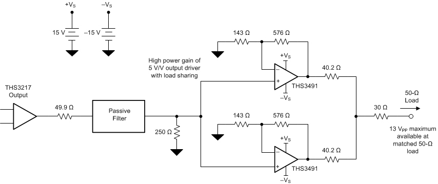
 Typical Arbitrary Waveform
Generator Output Drive Circuit
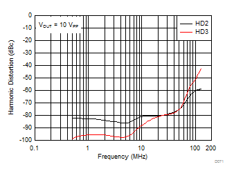
 Harmonic Distortion vs
Frequency