SLOS375B August 2014 – February 2024 THS4541
PRODUCTION DATA
- 1
- 1 Features
- 2 Applications
- 3 Description
- 4 Device Comparison Table
- 5 Pin Configuration and Functions
-
6 Specifications
- 6.1 Absolute Maximum Ratings
- 6.2 ESD Ratings
- 6.3 Recommended Operating Conditions
- 6.4 Thermal Information
- 6.5 Electrical Characteristics: (Vs+) – Vs– = 5 V
- 6.6 Electrical Characteristics: (Vs+) – Vs– = 3 V
- 6.7 Typical Characteristics 5-V Single Supply
- 6.8 Typical Characteristics: 3-V Single Supply
- 6.9 Typical Characteristics: 3-V to 5-V Supply Range
-
7 Parameter Measurement Information
- 7.1 Example Characterization Circuits
- 7.2 Frequency-Response Shape Factors
- 7.3 I/O Headroom Considerations
- 7.4 Output DC Error and Drift Calculations and the Effect of Resistor Imbalances
- 7.5 Noise Analysis
- 7.6 Factors Influencing Harmonic Distortion
- 7.7 Driving Capacitive Loads
- 7.8 Thermal Analysis
-
8 Detailed Description
- 8.1 Overview
- 8.2 Functional Block Diagram
- 8.3 Feature Description
- 8.4
Device Functional Modes
- 8.4.1
Operation from Single-Ended Sources to Differential Outputs
- 8.4.1.1 AC-Coupled Signal Path Considerations for Single-Ended Input to Differential Output Conversion
- 8.4.1.2 DC-Coupled Input Signal Path Considerations for Single-Ended to Differential Conversion
- 8.4.1.3 Resistor Design Equations for the Single-Ended to Differential Configuration of the FDA
- 8.4.1.4 Input Impedance for the Single-Ended to Differential FDA Configuration
- 8.4.2 Differential-Input to Differential-Output Operation
- 8.4.1
Operation from Single-Ended Sources to Differential Outputs
- 9 Application and Implementation
- 10Device and Documentation Support
- 11Revision History
- 12Mechanical, Packaging, and Orderable Information
Package Options
Refer to the PDF data sheet for device specific package drawings
Mechanical Data (Package|Pins)
- RUN|10
- RGT|16
Thermal pad, mechanical data (Package|Pins)
Orderable Information
7.5 Noise Analysis
Figure 7-10 shows that the first step in the output noise analysis is to reduce the application circuit to the simplest form with equal feedback and gain-setting elements to ground, with the FDA and resistor noise terms to be considered.
 Figure 7-10 FDA
Noise-Analysis Circuit
Figure 7-10 FDA
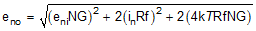
Noise-Analysis CircuitThe noise powers are shown for each term. When the Rf and Rg terms are matched on each side, the total differential output noise is the RSS of these separate terms. Equation 6 shows the total output noise using NG ≡ 1 + Rf / Rg. Each resistor noise term is a 4kTR power.
The first term is simply the differential input spot noise times the noise gain. The second term is the input current noise terms times the feedback resistor (and because there are two terms, the power is two times one of the terms). The last term is the output noise resulting from both the Rf and Rg resistors, again times two, for the output noise power of each side added together. Using the exact values for a 50-Ω, matched, single-ended to differential gain, sweep with a fixed Rf = 402 Ω (see Table 8-1) and the intrinsic noise eni = 2.2 nV and In = 1.9 pA for the THS4541, gives an output spot noise from Equation 6. Then, dividing by the signal gain (Av) gives the input-referred, spot-noise voltage (ei) shown in Table 7-5.
| Av | Rt, EXACT (Ω) | Rg1, EXACT (Ω) | Rg2, EXACT (Ω) | NOISE GAIN | eno (nV/√ Hz) | ei (nV/√ Hz) |
|---|---|---|---|---|---|---|
| 1 | 55.2 | 399 | 425 | 1.94 | 6.64 | 6.64 |
| 2 | 60.1 | 191 | 218 | 2.85 | 8.71 | 4.36 |
| 3 | 65.6 | 124 | 153 | 3.63 | 10.7 | 3.56 |
| 4 | 72 | 89.7 | 119 | 4.37 | 12.1 | 3.03 |
| 5 | 79.7 | 67.8 | 98.3 | 5.09 | 13.7 | 2.74 |
| 6 | 89.1 | 54.2 | 86.5 | 5.65 | 15.4 | 2.56 |
| 7 | 101 | 43.2 | 76.6 | 6.25 | 16.7 | 2.39 |
| 8 | 117 | 35.2 | 70.1 | 6.74 | 17.3 | 2.16 |
| 9 | 138 | 29.0 | 65.8 | 7.11 | 18.6 | 2.06 |
| 10 | 170 | 23.6 | 62.5 | 7.44 | 18.9 | 1.89 |
| 11 | 220 | 18.7 | 59.3 | 7.78 | 19.6 | 1.78 |
| 12 | 313 | 14.6 | 57.7 | 7.97 | 20.0 | 1.66 |
| 13 | 545 | 10.8 | 56.6 | 8.11 | 20.3 | 1.56 |
| 14 | 2209 | 7.26 | 56.1 | 8.16 | 21.1 | 1.50 |
Notice that the input-referred ei is less than 2.2 nV/√Hz for just the THS4541 above a gain of 7 V/V. This result is because NG is less than Av when the source impedance is included in the NG calculation.