SCPS268A September 2017 – February 2022 TIC10024-Q1
PRODUCTION DATA
- 1 Features
- 2 Applications
- 3 Description
- 4 Revision History
- 5 Pin Configuration and Functions
- 6 Specifications
- 7 Parameter Measurement Information
-
8 Detailed Description
- 8.1 Overview
- 8.2 Functional Block Diagram
- 8.3
Feature Description
- 8.3.1 VS Pin
- 8.3.2 VDD Pin
- 8.3.3 Device Initialization
- 8.3.4 Device Trigger
- 8.3.5 Device Reset
- 8.3.6 VS Under-Voltage (UV) Condition
- 8.3.7 VS Over-Voltage (OV) Condition
- 8.3.8 Switch Inputs Settings
- 8.3.9 Interrupt Generation and INT Assertion
- 8.3.10 Temperature Monitor
- 8.3.11 Parity Check And Parity Generation
- 8.3.12 Cyclic Redundancy Check (CRC)
- 8.4 Device Functional Modes
- 9 Programming
- 10Application and Implementation
- 11Power Supply Recommendations
- 12Layout
- 13Device and Documentation Support
- 14Mechanical, Packaging, and Orderable Information
Package Options
Mechanical Data (Package|Pins)
- DCP|38
Thermal pad, mechanical data (Package|Pins)
- DCP|38
Orderable Information
3 Description
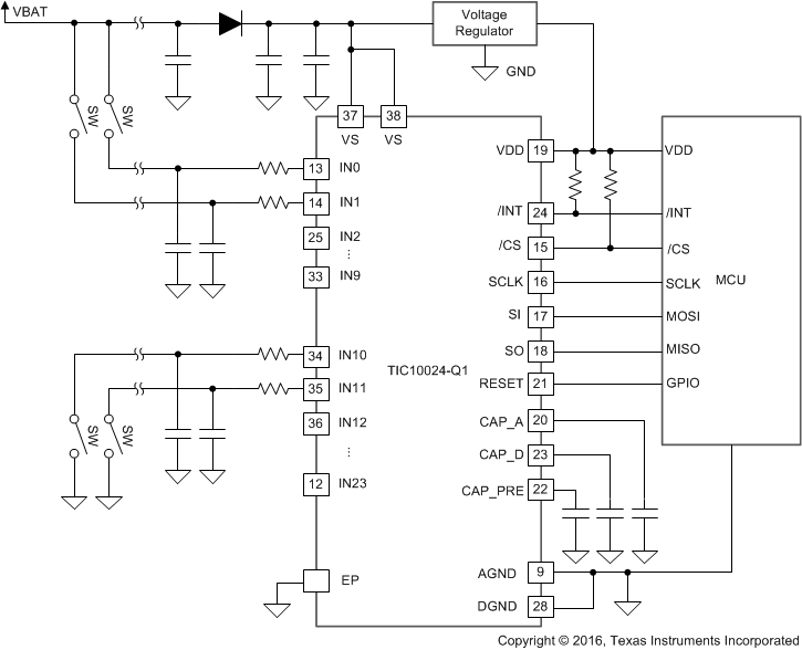
The TIC10024-Q1 is an advanced Multiple Switch Detection Interface (MSDI) device designed to detect external switch status in a 12-V automotive system. The TIC10024-Q1 features a comparator with adjustable thresholds to monitor digital switches independently of the MCU. The device monitors 24 direct switch inputs, with 10 inputs configurable to monitor switches connected to either ground or battery. There are 6 unique wetting current settings that can be programmed for each input to support different application scenarios. The device supports wake-up operation on all switch inputs to eliminate the need to keep the MCU active continuously, thus reducing power consumption of the system. The TIC10024-Q1 also offers integrated fault detection and ESD protection for improved system robustness. The TIC10024-Q1 supports 2 modes of operations: continuous and polling mode. In continuous mode, wetting current is supplied continuously. In polling mode, wetting current is turned on periodically to sample the input status based on a programmable timer, thus the system power consumption is significantly reduced.
| PART NUMBER | PACKAGE(1) | BODY SIZE (NOM) |
|---|---|---|
| TIC10024-Q1 | TSSOP (38) | 9.70 mm x 4.40 mm |
 Simplified Schematic