SLLSEV6C July 2017 – February 2021 TIOS101 , TIOS1013 , TIOS1015
PRODUCTION DATA
- 1 Features
- 2 Applications
- 3 Description
- 4 Revision History
- 5 Pin Configuration and Functions
- 6 Specifications
- 7 Parameter Measurement Information
-
8 Detailed Description
- 8.1 Overview
- 8.2 Functional Block Diagrams
- 8.3
Feature Description
- 8.3.1 Current Limit Configuration
- 8.3.2 Current Fault Detection, Indication and Auto Recovery
- 8.3.3 Thermal Warning, Thermal Shutdown
- 8.3.4 Fault Reporting (NFAULT)
- 8.3.5 Device Function Tables
- 8.3.6 The Integrated Voltage Regulator (LDO)
- 8.3.7 Reverse Polarity Protection
- 8.3.8 Integrated Surge Protection and Transient Waveform Tolerance
- 8.3.9 Power Up Sequence
- 8.3.10 Undervoltage Lock-Out (UVLO)
- 8.4 Device Functional Modes
- 9 Application Information Disclaimer
- 10Power Supply Recommendations
- 11Layout
- 12Device and Documentation Support
Package Options
Mechanical Data (Package|Pins)
- DMW|10
Thermal pad, mechanical data (Package|Pins)
Orderable Information
9.2.3 Application Curves
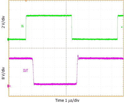
| 125 kHz |
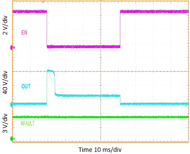
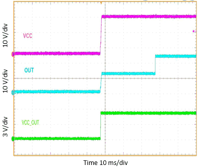 Figure 9-6 OUT Power Up Delay, High Side Mode
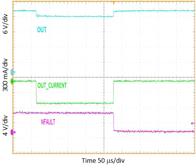 Figure 9-8 OUT In Current Fault, High Side Mode
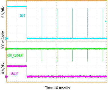 Figure 9-10 OUT In Current Fault Auto Recovery, High Side Mode
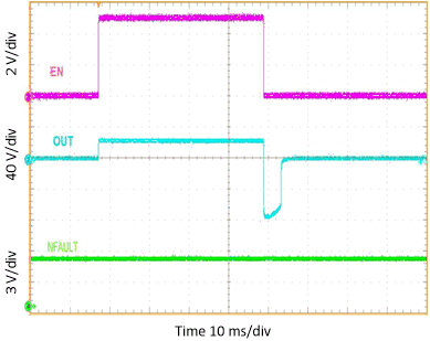
| 1.5-H Inductor | With = 100 Ω | RSET = OPEN |
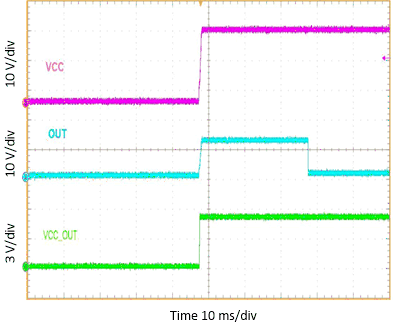 Figure 9-5 OUT Power Up Delay, Low Side Mode
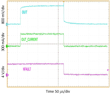 Figure 9-7 OUT In Current Fault, Low Side Mode
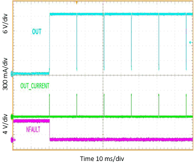 Figure 9-9 OUT In Current Fault Auto Recovery, Low Side Mode
| 1.5-H Inductor | With = 100 Ω | RSET = OPEN |